|
|
|
PDF AD5680 Data sheet ( Hoja de datos )
| Número de pieza | AD5680 | |
| Descripción | 5 V 18-Bit nanoDAC | |
| Fabricantes | Analog Devices | |
| Logotipo | ||
Hay una vista previa y un enlace de descarga de AD5680 (archivo pdf) en la parte inferior de esta página. Total 20 Páginas | ||
|
No Preview Available !
www.DataSheet4U.com
FEATURES
Single 18-bit nanoDAC
18-bit monotonic
12-bit accuracy guaranteed
Tiny 8-lead SOT-23 package
Power-on reset to zero scale/midscale
4.5 V to 5.5 V power supply
Serial interface
Rail-to-rail operation
SYNC interrupt facility
Temperature range −40°C to +105°C
APPLICATIONS
Closed-loop process control
Low bandwidth data acquisition systems
Portable battery-powered instruments
Gain and offset adjustment
Precision setpoint control
GENERAL DESCRIPTION
The AD5680, a member of the nanoDAC family, is a single,
18-bit buffered voltage-out DAC that operates from a single
4.5 V to 5.5 V supply and is 18-bit monotonic.
The AD5680 requires an external reference voltage to set the
output range of the DAC. The part incorporates a power-on
reset circuit that ensures the DAC output powers up to 0 V
(AD5680-1) or to midscale (AD5680-2) and remains there until
a valid write takes place.
The low power consumption of this part in normal operation
makes it ideally suited to portable battery-operated equipment.
The power consumption is 1.6 mW at 5 V.
The AD5680 on-chip precision output amplifier allows rail-to-
rail output swing to be achieved. For remote sensing applications,
the output amplifier’s inverting input is available to the user.
The AD5680 uses a versatile 3-wire serial interface that operates
at clock rates up to 30 MHz, and is compatible with standard
SPI®, QSPI™, MICROWIRE™, and DSP interface standards.
5 V 18-Bit nanoDACTM
in a SOT-23
AD5680
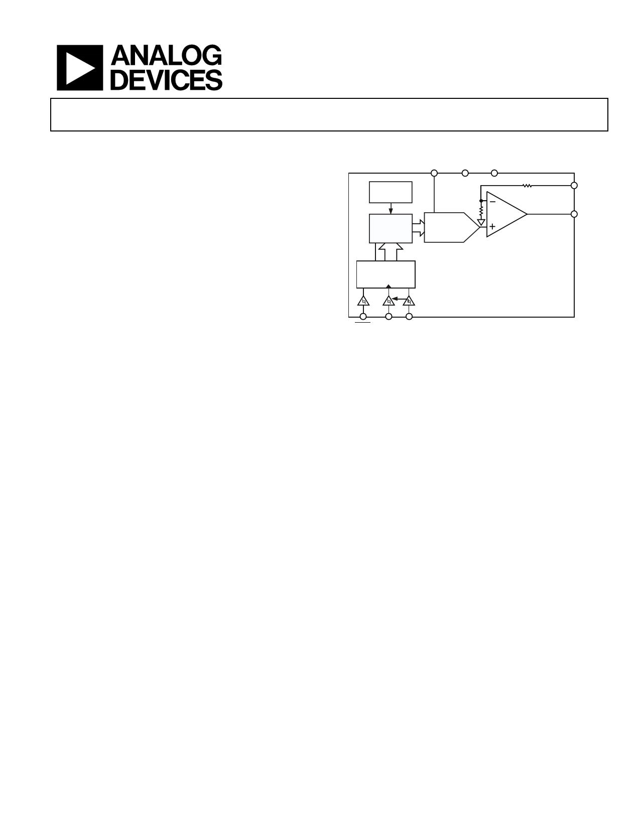
FUNCTIONAL BLOCK DIAGRAM
VREF
GND
VDD
POWER-ON
RESET
DAC
REGISTER
REF(+)
18-BIT
DAC
OUTPUT
BUFFER
VFB
VOUT
INPUT
CONTROL
LOGIC
SYNC SCLK DIN
Figure 1.
AD5680
PRODUCT HIGHLIGHTS
1. 18 bits of resolution.
2. 12-bit accuracy guaranteed for 18-bit DAC.
3. Available in an 8-lead SOT-23.
4. Low power. Typically consumes 1.6 mW at 5 V.
5. Power-on reset to zero scale or to midscale.
RELATED DEVICES
AD5662 16-bit DAC in SOT-23.
Rev. 0
Information furnished by Analog Devices is believed to be accurate and reliable. However, no
responsibility is assumed by Analog Devices for its use, nor for any infringements of patents or other
rights of third parties that may result from its use. Specifications subject to change without notice. No
license is granted by implication or otherwise under any patent or patent rights of Analog Devices.
Trademarksandregisteredtrademarksarethepropertyoftheirrespectiveowners.
One Technology Way, P.O. Box 9106, Norwood, MA 02062-9106, U.S.A.
Tel: 781.329.4700
www.analog.com
Fax: 781.461.3113
©2006 Analog Devices, Inc. All rights reserved.
1 page 
ABSOLUTE MAXIMUM RATINGS
TA = 25°C, unless otherwise noted.
Table 3.
Parameter
VDD to GND
VOUT to GND
VFB to GND
VREF to GND
Digital Input Voltage to GND
Operating Temperature Range
Industrial (B Version)
Storage Temperature Range
Junction Temperature (TJ max)
Power Dissipation
SOT-23 Package (4-Layer Board)
θJA Thermal Impedance
Reflow Soldering Peak Temperature
Pb-free
Rating
−0.3 V to +7 V
−0.3 V to VDD + 0.3 V
−0.3 V to VDD + 0.3 V
−0.3 V to VDD + 0.3 V
−0.3 V to VDD + 0.3 V
−40°C to +105°C
−65°C to +150°C
150°C
(TJ max − TA)/θJA
119°C/W
260°C
AD5680
Stresses above those listed under Absolute Maximum Ratings
may cause permanent damage to the device. This is a stress
rating only; functional operation of the device at these or any
other conditions above those indicated in the operational
section of this specification is not implied. Exposure to absolute
maximum rating conditions for extended periods may affect
device reliability.
ESD CAUTION
ESD (electrostatic discharge) sensitive device. Electrostatic charges as high as 4000 V readily accumulate on the
human body and test equipment and can discharge without detection. Although this product features
proprietary ESD protection circuitry, permanent damage may occur on devices subjected to high energy
electrostatic discharges. Therefore, proper ESD precautions are recommended to avoid performance
degradation or loss of functionality.
Rev. 0 | Page 5 of 20
5 Page 
THEORY OF OPERATION
DAC SECTION
The AD5680 DAC is fabricated on a CMOS process. The
architecture consists of a string DAC followed by an output
buffer amplifier. Figure 22 shows a block diagram of the DAC
architecture.
DAC REGISTER
VDD
REF (+)
RESISTOR
STRING
REF (–)
R
GND
Figure 22. DAC Architecture
R
VFB
VOUT
OUTPUT
AMPLIFIER
Because the input coding to the DAC is straight binary, the ideal
output voltage is given by
VOUT
= VREF
×
⎜⎝⎛
D
262144
⎟⎠⎞
where D is the decimal equivalent of the binary code that is
loaded to the DAC register. It can range from 0 to 262143.
RESISTOR STRING
The resistor string section is shown in Figure 23. It is simply a
string of resistors, each of value R. The code loaded to the DAC
register determines at which node on the string the voltage is
tapped off to be fed into the output amplifier. The voltage is
tapped off by closing one of the switches connecting the string
to the amplifier. Because it is a string of resistors, it is guaranteed
monotonic.
R
R
R TO OUTPUT
AMPLIFIER
R
R
Figure 23. Resistor String
AD5680
OUTPUT AMPLIFIER
The output buffer amplifier can generate rail-to-rail voltages on
its output, which gives an output range of 0 V to VDD. This output
buffer amplifier has a gain of 2 derived from a 50 kΩ resistor
divider network in the feedback path. The output amplifier’s
inverting input is available to the user, allowing for remote
sensing. This VFB pin must be connected to VOUT for normal
operation. It can drive a load of 2 kΩ in parallel with 1000 pF to
GND. The source and sink capabilities of the output amplifier can
be seen in Figure 9. The slew rate is 1.5 V/μs with a ¼ to ¾ full-
scale settling time of 10 μs.
INTERPOLATOR ARCHITECTURE
The AD5680 contains a 16-bit DAC with an internal clock
generator and interpolator. The voltage levels generated by the
16-bit, 1 LSB step can be subdivided using the interpolator to
increase the resolution to 18 bits.
The 18-bit input code can be divided into two segments:
16-bit DAC code (DB19 to DB4) and 2-bit interpolator code
(DB3 and DB2). The input to the DAC is switched between a
16-bit code (for example, Code 1023) and a 16-bit code + 1 LSB
(for example, Code 1024). The 2-bit interpolator code deter-
mines the duty cycle of the switching and hence the 18-bit
code level. See Table 5 for an example.
Table 5.
18-Bit Code
DB19 to DB2
4092
4093
4094
4095
4096
16-Bit
DAC Code
DB19 to DB4
1023
1023
1023
1023
1024
2-Bit
Interpolator Code
DB3 DB2
00
01
10
11
00
Duty Cycle
0
25%
50%
75%
0
The DAC output voltage is given by the average value of
the waveform switching between 16-bit code (C) and 16-bit
code + 1 (C + 1). The output voltage is a function of the duty
cycle of the switching.
18-BIT INPUT CODE
C
18 16 C + 1
+1
MUX
16
2 INTERPOLATOR
CLK
DAC
C+1
C
C+1
C
C+1
C
VOUT
FILTER
PLANT
75% DUTY CYCLE
50% DUTY CYCLE
25% DUTY CYCLE
Figure 24. Interpolation Architecture
Rev. 0 | Page 11 of 20
11 Page | ||
| Páginas | Total 20 Páginas | |
| PDF Descargar | [ Datasheet AD5680.PDF ] | |
Hoja de datos destacado
| Número de pieza | Descripción | Fabricantes |
| AD568 | 12-Bit Ultrahigh Speed Monolithic D/A Converter | Analog Devices |
| AD5680 | 5 V 18-Bit nanoDAC | Analog Devices |
| AD5681R | Tiny 16-/14-/12-Bit SPI nanoDAC+ | Analog Devices |
| AD5682R | Tiny 16-/14-/12-Bit SPI nanoDAC+ | Analog Devices |
| Número de pieza | Descripción | Fabricantes |
| SLA6805M | High Voltage 3 phase Motor Driver IC. |
Sanken |
| SDC1742 | 12- and 14-Bit Hybrid Synchro / Resolver-to-Digital Converters. |
Analog Devices |
|
DataSheet.es es una pagina web que funciona como un repositorio de manuales o hoja de datos de muchos de los productos más populares, |
| DataSheet.es | 2020 | Privacy Policy | Contacto | Buscar |