|
|
|
PDF NCP1381 Data sheet ( Hoja de datos )
| Número de pieza | NCP1381 | |
| Descripción | Low Standby High Performance PWM Controller | |
| Fabricantes | ON Semiconductor | |
| Logotipo | ||
Hay una vista previa y un enlace de descarga de NCP1381 (archivo pdf) en la parte inferior de esta página. Total 26 Páginas | ||
|
No Preview Available !
www.DataSheet4U.com
NCP1381
Low−Standby High
Performance PWM
Controller
Housed in a SO−14 package, the NCP1381 includes everything
needed to build rugged and efficient Quasi−Resonant (QR) Switching
Power Supplies. When powered by a front−end Power Factor
Correction circuitry, the NCP1381 automatically disconnects the PFC
controller in low output loading conditions (with an adjustable level),
thus improving the standby power. This is particularly well suited for
medium to high power offline applications, e.g. notebook adapters.
When the current setpoint falls below a given value, e.g. the output
power demand diminishes, the IC automatically enters the so−called
skip cycle mode and provides excellent efficiency at light loads.
Because this occurs at an adjustable low peak current together with a
proprietary Soft−Skipt technique, no acoustic noise takes place. Skip
cycle also offers the ability to easily select the maximum switching
frequency at which foldback and standby take place.
The NCP1381 also features several efficient protection options like
a) a short−circuit / overload detection independent of the auxiliary
voltage b) an auto−recovery brown−out detection and c) an input to
externally latch the circuit in case of Overvoltage Protection or Over
Temperature Protection.
Features
• Current−Mode Quasi−Resonant Operation
• Adjustable Line Over Power Protection
• Extremely Low Startup Current of 15 mA Maximum
• Soft−Skip Cycle Capability at Adjustable Peak Currents
• Plateau Sensing Overvoltage
• Brown−Out Protection
• Maximum tON Limitation
• Overpower Protection by current Sense Offset
• Internal 5 ms Soft−Start Management
• Short−Circuit Protection Independent from Auxiliary Level
• External Latch Input Pin for an OTP Signal
• Go−To−Standby Signal for the PFC Front Stage
• True Frequency (tON + tOFF) Clamp Circuit
• Low and Noiseless, No−Load Standby Power
• Internal Leading Edge Blanking
• +500 mA / −800 mA Peak Current Drive Capability
• 5 V / 10 mA Reference Voltage
• This is a Pb−Free Device
Typical Applications
• High Power AC/DC Adapters for Notebooks, etc
• Offline Battery Chargers
• Set−Top Boxes Power Supplies, TV, Monitors, etc
http://onsemi.com
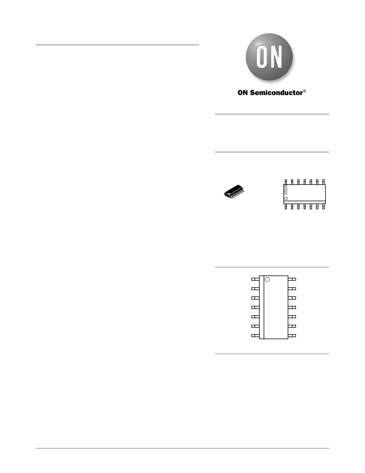
HIGH PERFORMANCE QR
CONTROLLER FEATURING PFC
SHUTDOWN
14
1
MARKING
DIAGRAM
14
SOIC−14
D SUFFIX
CASE 751A
1
NCP1381G
AWLYWW
NCP1381G = Specific Device Code
A = Assembly Location
WL = Wafer Lot
Y = Year
WW = Work Week
G = Pb−Free Package
ADJ_GTS
BO
DMG
Timer
Skip/OVP
FB
CS
1
2
3
4
5
6
7
14 nc
13 nc
12 Ref
11 GTS
10 VCC
9 DRV
8 GND
ORDERING INFORMATION
See detailed ordering and shipping information in the package
dimensions section on page 25 of this data sheet.
© Semiconductor Components Industries, LLC, 2006
July, 2006 − Rev. 3
1
Publication Order Number:
NCP1381/D
1 page 
NCP1381
ELECTRICAL CHARACTERISTICS
(For typical values TJ = 25°C, for min/max values TJ = 0°C to +125°C, VCC = 12 V unless otherwise noted)
Symbol
Rating
Pin Min
CURRENT COMPARATOR
Sskip Typical Internal Soft−start period when Leaving Skip
GO−TO−STANDBY
− 100
RGTS
Pin 11 Output Impedance (or Rdson between Pin 10 and Pin 11 when SW
is Closed)
11
−
Rskip
Vskip
Hyst_ratio
Skip Adjustment Output Impedance
Default Skip Cycle Level
Ratio Between the Skip Level and the Skip Comparator Hysteresis
5 17
5−
−−
ADJ_GTS Threshold of the ADJ_GTS Comparator
1 220
Ihyst Internal Current Source that Creates an Adjustable Hysteresis to the
ADJ_GTS Comparator
1 4.0
DEMAGNETIZATION DETECTION BLOCK
Vth
VH
VCH
VCL
Tdem
Cpar
Rdown
Input Threshold Voltage (Vpin 3 Decreasing)
Hysteresis (Vpin 3 Increasing)
Input Clamp Voltage
High State (Ipin 3 = 3.0 mA)
Low State (Ipin 3 = −3.0 mA)
DMG Propagation Delay
Internal Input Capacitance at Vpin 3 = 1 V
Internal Pulldown Resistor
3 30
3−
39
3 −0.9
3−
3−
3 20
Tblank Internal Blanking Delay after TON
Tsw−(min) Frequency Clamp, Minimum (TON + TOFF)
FEEDBACK SECTION
3−
− 7.0
Rup Internal Pullup Resistor
Iratio Pin 6 to Current Setpoint Division Ratio (Maximum VFB = 5 V)
Ref Voltage Reference, Iload = 1 mA
Iref Reference Maximum Output Current
PROTECTIONS
6 7.5
−−
12 4.75
12 10
Vzenlatch VCC Limitation in Latched Fault Mode
MaxtON Maximum On Time Duration
Itimer
Timer Charging Current
Vtimfault Timer Fault Validation Level
Tdelay Timeout Before Validating Short−circuit or GTS, Ct = 0.22 mF
Vlatchdem Latching Level On the Demagnetization Input
Tsamp Sampling Time for Vlatchdem Detection after the End of the TON
Vlatch Latchoff Level On the Skip Adjustment Pin
TDELLATCH Propagation Delay from Latch Detected to Gate Turned Off (Pin 9
Loaded by 1 nF)
10 −
9−
4 7.0
4 3.5
−−
3 3.7
3−
5 3.15
−−
VBOhigh
VBOlow
IBO
TSD
TSDhyst
Brown−out Level High
Brown−out Level Low
Brown−out Pin Input Bias Current
Temperature Shutdown, Maximum Value
Hysteresis While in Temperature Shutdown
2 0.45
2 0.21
2−
− 140
−−
Typ
175
15
25
800
3.4
250
5.0
50
30
10
−0.7
200
10
30
3.5
8.0
10
4.0
5.0
−
6.0
45
10
4.0
90
4.1
4.0
3.5
220
0.5
0.24
0.04
−
30
Max
250
−
35
−
−
280
6.0
80
−
12
−0.5
−
−
45
−
9.0
12.5
−
5.25
−
−
−
13
4.5
−
4.5
−
3.85
−
0.55
0.275
−
−
−
Unit
ms
W
kW
mV
−
mV
mA
mV
mV
V
V
ns
pF
kW
ms
ms
kW
V
mA
V
ms
mA
V
ms
V
ms
V
ns
V
V
mA
°C
°C
http://onsemi.com
5
5 Page 
S
VDD
DQ
CLK Q
R
Demag
2
NCP1381
VDD
+
−
+
3 ms
Blanking
−
+
+
45 mV
Prioritary
Reset
D
S
Q
DRV
CLK Q
R
DRV
DRV
VDD
+
−
+
One
Shot
VDD
+
−
+
Skip ILimit
Reset Reset
Fault
Figure 9. Internal QR Architecture
7.00
5.00
Possible
Restart
3.00
1.00
−1.00
0V
45 mV
Figure 10. Core Reset Detection is Done Through the
Monitoring of a Dedicated Auxiliary Winding
Skipping Cycle Mode
The NCP1381 automatically skips switching cycles when
the output power demand drops below a given level. This is
accomplished by monitoring the FB pin. In normal
operation, pin 6 imposes a peak current accordingly to the
load value. If the load demand decreases, the internal loop
asks for less peak current. When this setpoint reaches a
determined level, the IC prevents the current from
decreasing further down and starts to blank the output
pulses: the IC enters the so−called skip cycle mode, also
named controlled burst operation. The power transfer now
depends upon the width of the pulse bunches (Figure 11) and
follows the following formula:
1
2
@
LP
@
IP2
@
Fsw
@
Dburst
(eq. 1)
with
LP = Primary Inductance
Fsw = Switching Frequency Within the Burst
IP = Peak Current at which Skip Cycle Occurs
Dburst = Burst Width/Burst Recurrence
http://onsemi.com
11
11 Page | ||
| Páginas | Total 26 Páginas | |
| PDF Descargar | [ Datasheet NCP1381.PDF ] | |
Hoja de datos destacado
| Número de pieza | Descripción | Fabricantes |
| NCP1380 | Quasi-Resonant Current Mode Controller | ON Semiconductor |
| NCP1381 | Low Standby High Performance PWM Controller | ON Semiconductor |
| Número de pieza | Descripción | Fabricantes |
| SLA6805M | High Voltage 3 phase Motor Driver IC. |
Sanken |
| SDC1742 | 12- and 14-Bit Hybrid Synchro / Resolver-to-Digital Converters. |
Analog Devices |
|
DataSheet.es es una pagina web que funciona como un repositorio de manuales o hoja de datos de muchos de los productos más populares, |
| DataSheet.es | 2020 | Privacy Policy | Contacto | Buscar |