|
|
|
PDF AD15252 Data sheet ( Hoja de datos )
| Número de pieza | AD15252 | |
| Descripción | Dual ADC | |
| Fabricantes | Analog Devices | |
| Logotipo | ||
Hay una vista previa y un enlace de descarga de AD15252 (archivo pdf) en la parte inferior de esta página. Total 20 Páginas | ||
|
No Preview Available !
www.DataSheet4U.com
FEATURES
12-bit, 65 MSPS dual ADC
Differential input with 100 Ω input impedance
Full-scale analog input: 296 mV p-p
170 MHz, 3 dB bandwidth
SNR (−9 dBFS): 64 dBFS (70 MHz AIN), 64 dBFS (140 MHz AIN)
SFDR (−9 dBFS): 77 dBFS (70 MHz AIN), 73 dBFS (140 MHz AIN)
435 mW per channel
Dual parallel output buses
Out-of-range indicators
Independent clocks
Duty cycle stabilizer
Twos complement or offset binary data format
APPLICATIONS
Antijam GPS receivers
Wireless and wired broadband communications
Communications test equipment
12-Bit, 65 MSPS, Dual ADC
AD15252
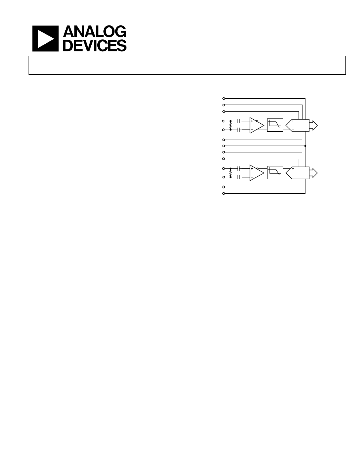
FUNCTIONAL BLOCK DIAGRAM
OTR_A
PDWNA
CLKA
AD15252
INA
OEB_A
DFS
PDWNB
CLKB
INB
OEB_B
OTR_B
LPF
LPF
Figure 1.
DATA
BUS A
DATA
BUS B
GENERAL DESCRIPTION
The AD15252 is a dual, 12-bit, 65 MSPS, analog-to-digital
converter (ADC). It features a differential front-end
amplification circuit followed by a sample-and-hold amplifier
and multistage pipeline ADC. It is designed to operate with a
3.3 V analog supply and a 2.5 V/3.3 V digital supply. Each input
is fully differential, ac-coupled, and terminated in 100 Ω input
impedances. The full-scale differential signal input range is
296 mV p-p.
Two parallel, 12-bit digital output buses provide data flow from
the ADCs. The digital output data is presented in either straight
binary or twos complement format. Out-of-range (OTR) signals
indicate an overflow condition, which can be used with the
most significant bit to determine low or high overflow. Dual
single-ended clock inputs control all internal conversion cycles.
A duty cycle stabilizer allows wide variations in the clock duty
cycle while maintaining excellent performance. The AD15252 is
optimized for applications in antijam global positioning
receivers and is well suited for communications applications.
PRODUCT HIGHLIGHTS
1. Dual 12-bit, 65 MSPS ADC with integrated analog signal
conditioning optimized for antijam global positioning
system receiver (AJ-GPS) applications.
2. Operates from a single 3.3 V power supply and features a
separate digital output driver supply to accommodate 2.5 V
and 3.3 V logic families.
3. Packaged in a space-saving 8 mm × 8 mm chip scale
package ball grid array (CSP_BGA) and is specified over
the industrial temperature range (–40°C to +85°C).
Rev. 0
Information furnished by Analog Devices is believed to be accurate and reliable.
However, no responsibility is assumed by Analog Devices for its use, nor for any
infringements of patents or other rights of third parties that may result from its use.
Specifications subject to change without notice. No license is granted by implication
or otherwise under any patent or patent rights of Analog Devices. Trademarks and
registered trademarks are the property of their respective owners.
One Technology Way, P.O. Box 9106, Norwood, MA 02062-9106, U.S.A.
Tel: 781.329.4700
www.analog.com
Fax: 781.461.3113 © 2005 Analog Devices, Inc. All rights reserved.
1 page 
ABSOLUTE MAXIMUM RATINGS
Table 3.
Parameter
AVDD to AGND
DRVDD to DRGND
DRGND to AGND
DRVDD to AVDD
Analog Inputs
Digital Outputs
CLK
Operational Case Temperature
Storage Temperature Range
Lead Temperature: Infrared, 15 sec
Rating
−0.3 V, +3.9 V
−0.3 V, +3.9 V
−0.3 V, +0.3 V
−3.9 V, +3.9 V
−0.3 V, AVDD + 0.3 V
−0.3 V, DRVDD + 0.3 V
−0.3 V, AVDD + 0.3 V
−40°C to 85°C
−65°C to 150°C
230°C
AD15252
Stresses above those listed under Absolute Maximum Ratings
may cause permanent damage to the device. This is a stress
rating only; functional operation of the device at these or any
other conditions above those indicated in the operational
section of this specification is not implied. Exposure to absolute
maximum rating conditions for extended periods may affect
device reliability.
ESD CAUTION
ESD (electrostatic discharge) sensitive device. Electrostatic charges as high as 4000 V readily accumulate on
the human body and test equipment and can discharge without detection. Although this product features
proprietary ESD protection circuitry, permanent damage may occur on devices subjected to high energy
electrostatic discharges. Therefore, proper ESD precautions are recommended to avoid performance
degradation or loss of functionality.
Rev. 0 | Page 5 of 20
5 Page 
AD15252
THEORY OF OPERATION
The AD15252 consists of two high performance ADC channels.
The dual ADC paths are independent, except for a shared
internal band gap reference source, VREF. Each path consists of
a differential front end amplification circuit followed by a
sample-and-hold amplifier and multistage pipeline ADC.
The output-staging block aligns the data, carries out the error
correction, and passes the data to the output buffers. The output
buffers are powered from a separate supply, allowing adjustment
of the output voltage swing.
ANALOG INPUT
Each analog input is fully differential, allowing sampling of
differential input signals. The differential input signals are ac-
coupled and terminated in 100 Ω input impedances. The full-
scale differential signal input range is 296 mV p-p.
VOLTAGE REFERENCE
The internal voltage reference of the ADC is pin strapped to a
fixed value of 0.5 V. A 10 μF capacitor should be used between
REFT and REFB.
CLOCK INPUT AND CONSIDERATIONS
Typical high speed ADCs use both clock edges to generate a
variety of internal timing signals and, as a result, can be
sensitive to clock duty cycle. Commonly, a 5% tolerance is
required on the clock duty cycle to maintain dynamic
performance characteristics.
The AD15252 provides separate clock inputs for each channel.
The optimum performance is achieved with the clocks operated
at the same frequency and phase. Clocking the channels
asynchronously can significantly degrade performance. In some
applications, it is desirable to skew the clock timing of adjacent
channels. The AD15252’s separate clock inputs allow clock
timing skew (typically ±1 ns) between the channels without
significant performance degradation.
The AD15252 contains two internal clock duty cycle stabilizers
(DCS), one for each converter, which retime the nonsampling
edge, providing an internal clock with a nominal 50% duty
cycle. Input clock rates of over 40 MHz can use the DCS so that
a wide range of input clock duty cycles can be accommodated.
Maintaining a 50% duty cycle clock is particularly important in
high speed applications, when proper track-and-hold times for
the converter are required to maintain high performance.
The duty cycle stabilizer uses a delay-locked loop to create the
nonsampling edge. As a result, any change to the sampling
frequency requires approximately 2 μs to 3 μs to allow the DLL
to acquire and settle to the new rate.
High speed, high resolution ADCs are sensitive to the quality of
the clock input. The degradation in SNR at a given full-scale
input frequency (fINPUT) due only to aperture jitter (tJ) can be
calculated by
SNR Degradation = 20 × log 10 (1/2 × p × f INPUT × tJ)
In the equation, the rms aperture jitter, tJ, represents the root-
sum square of all jitter sources, which includes the clock input,
analog input signal, and ADC aperture jitter specification.
Undersampling applications are particularly sensitive to jitter.
For optimal performance, especially in cases where aperture
jitter can affect the dynamic range of the AD15252, it is
important to minimize input clock jitter. The clock input
circuitry should use stable references, for example, using analog
power and ground planes to generate the valid high and low
digital levels for the AD15252 clock input. Power supplies for
clock drivers should be separated from the ADC output driver
supplies to avoid modulating the clock signal with digital noise.
Low jitter crystal-controlled oscillators make the best clock
sources. If the clock is generated from another type of source
(by gating, dividing, or other methods), it should be retimed by
the original clock at the last step.
POWER DISSIPATION AND STANDBY MODE
The power dissipated by the AD15252 is proportional to its
sampling rates. The digital (DRVDD) power dissipation is
determined primarily by the strength of the digital drivers and
the load on each output bit. The digital drive current can be
calculated by
IDRVDD = VDRVDD × CLOAD × fCLOCK × N
where:
N is the number of bits changing.
CLOAD is the average load on the digital pins that changed.
The analog circuitry is optimally biased so that each speed
grade provides excellent performance while affording reduced
power consumption. Each speed grade dissipates a baseline
power at low sample rates that increase with clock frequency.
Either channel of the AD15252 can be placed into standby mode
independently by asserting the PDWN_A or PDWN_B pins.
The minimum standby power is achieved when both channels
are placed into full power-down mode using PDWN_A =
PDWN_B = high. Under this condition, the internal references
are powered down. When either or both of the channel paths
are enabled after a power-down, the wake-up time is directly
related to the recharging of the REFT and REFB decoupling
capacitors and to the duration of the power-down. Typically, it
takes approximately 5 ms to restore full operation with fully
discharged 10 μF decoupling capacitors on REFT and REFB.
Rev. 0 | Page 11 of 20
11 Page | ||
| Páginas | Total 20 Páginas | |
| PDF Descargar | [ Datasheet AD15252.PDF ] | |
Hoja de datos destacado
| Número de pieza | Descripción | Fabricantes |
| AD15252 | Dual ADC | Analog Devices |
| Número de pieza | Descripción | Fabricantes |
| SLA6805M | High Voltage 3 phase Motor Driver IC. |
Sanken |
| SDC1742 | 12- and 14-Bit Hybrid Synchro / Resolver-to-Digital Converters. |
Analog Devices |
|
DataSheet.es es una pagina web que funciona como un repositorio de manuales o hoja de datos de muchos de los productos más populares, |
| DataSheet.es | 2020 | Privacy Policy | Contacto | Buscar |