|
|
|
PDF AD9981 Data sheet ( Hoja de datos )
| Número de pieza | AD9981 | |
| Descripción | High Performance 10-Bit Display Interface | |
| Fabricantes | Analog Devices | |
| Logotipo | ||
Hay una vista previa y un enlace de descarga de AD9981 (archivo pdf) en la parte inferior de esta página. Total 30 Páginas | ||
|
No Preview Available !
www.DataSheet4U.com
FEATURES
10-bit analog-to-digital converter
95 MSPS maximum conversion rate
9% or less p-p PLL clock jitter at 95 MSPS
Automated offset adjustment
2:1 input mux
Power-down via dedicated pin or serial register
4:4:4, 4:2:2, and DDR output format modes
Variable output drive strength
Odd/even field detection
External clock input
Regenerated Hsync output
Programmable output high impedance control
Hsyncs per Vsyncs counter
Pb-free package
APPLICATIONS
Advanced TVs
Plasma display panels
LCDTV
HDTV
RGB graphics processing
LCD monitors and projectors
Scan converters
GENERAL DESCRIPTION
The AD9981 is a complete, 10-bit, 95 MSPS, monolithic analog
interface optimized for capturing YPbPr video and RGB
graphics signals. Its 95 MSPS encode rate capability and full-
power analog bandwidth of 200 MHz supports all HDTV
video modes and graphics resolutions up to XGA (1024 × 768
at 85 Hz).
The AD9981 includes a 95 MHz triple ADC with an internal
reference, a PLL, programmable gain, offset, and clamp controls.
The user provides only 3.3 V and 1.8 V power supplies and an
analog input. Three-state CMOS outputs may be powered from
1.8 V to 3.3 V.
The AD9981’s on-chip PLL generates a sample clock from
the three-level sync (for YPbPr video) or the horizontal sync
(for RGB graphics). Sample clock output frequencies range from
10 MHz to 95 MHz. PLL clock jitter is 9% or less p-p typical at
95 MSPS.
Rev. 0
Information furnished by Analog Devices is believed to be accurate and reliable.
However, no responsibility is assumed by Analog Devices for its use, nor for any
infringements of patents or other rights of third parties that may result from its use.
Specifications subject to change without notice. No license is granted by implication
or otherwise under any patent or patent rights of Analog Devices. Trademarks and
registered trademarks are the property of their respective owners.
High Performance
10-Bit Display Interface
AD9981
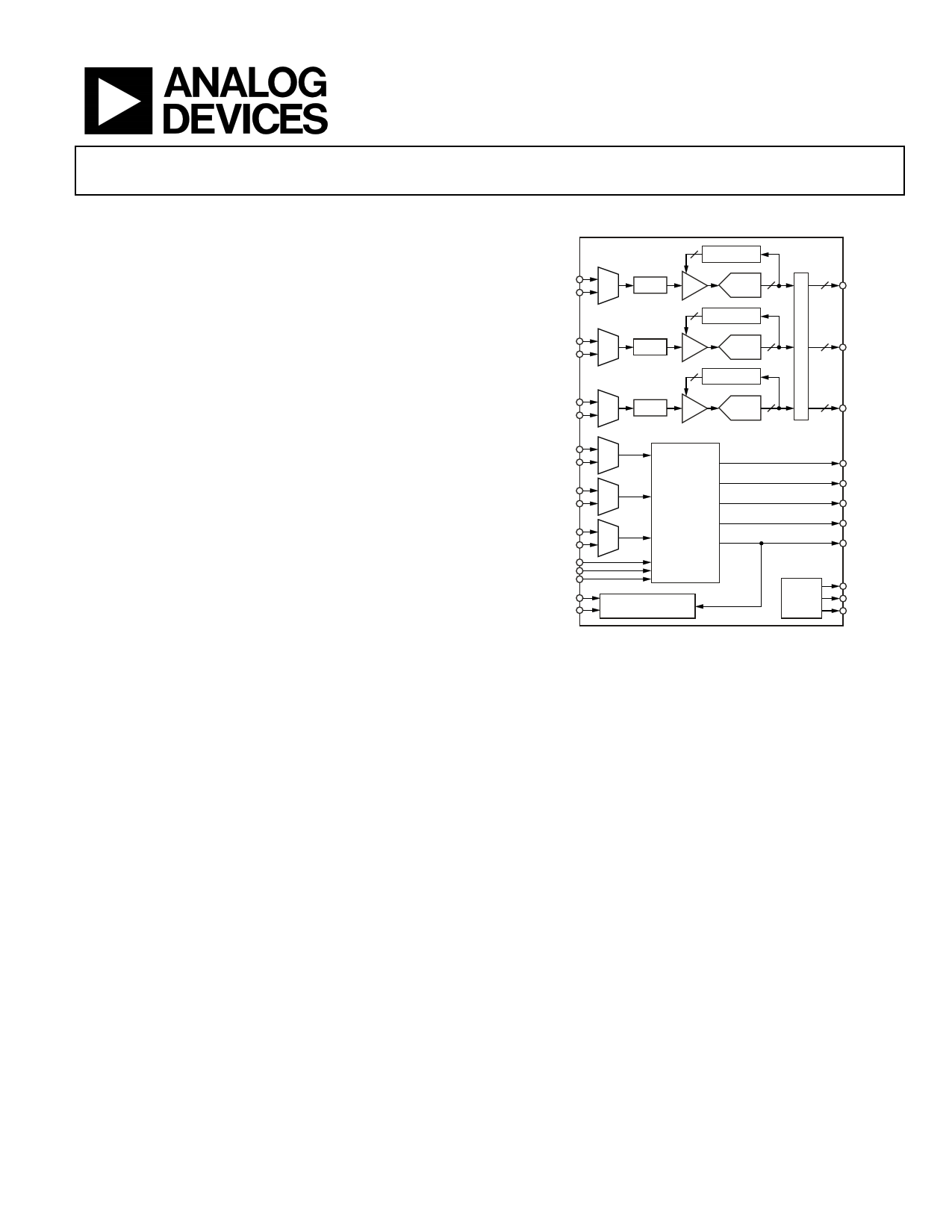
FUNCTIONAL BLOCK DIAGRAM
PR/REDIN1
PR/REDIN0
2:1
MUX
CLAMP
10
AUTO OFFSET
PGA
10-BIT 10
ADC
10
AUTO OFFSET
AD9981
10
REDOUT
Y/GREENIN1
Y/GREENIN0
2:1
MUX
CLAMP
PGA
10-BIT 10
ADC
10
AUTO OFFSET
10
GREENOUT
PB/BLUEIN1
PB/BLUEIN0
2:1
MUX
CLAMP
PGA
10-BIT 10
ADC
10
BLUEOUT
HSYNC1
HSYNC2
VSYNC1
VSYNC2
SOGIN1
SOGIN2
EXTCLK/COAST
CLAMP
FILT
SDA
SCL
2:1
MUX
2:1
MUX
2:1
MUX
SYNC
PROCESSING
PLL
POWER
MANAGEMENT
SERIAL REGISTER
Figure 1.
DATACK
SOGOUT
O/E FIELD
HSOUT
VSOUT/A0
VOLTAGE
REFS
REFHI
REFCM
REFLO
With internal Coast generation, the PLL maintains its output
frequency in the absence of sync input. A 32-step sampling
clock phase adjustment is provided. Output data, sync, and
clock phase relationships are maintained.
The auto-offset feature can be enabled to automatically restore
the signal reference levels and to automatically calibrate out any
offset differences between the three channels. The AD9981 also
offers full sync processing for composite sync and sync-on-
green applications. A clamp signal is generated internally or
may be provided by the user through the CLAMP input pin.
Fabricated in an advanced CMOS process, the AD9981 is
provided in a space-saving, 80-pin, Pb-free, LQFP surface
mount plastic package. It is specified over the 0°C to +70°C
temperature range.
One Technology Way, P.O. Box 9106, Norwood, MA 02062-9106, U.S.A.
Tel: 781.329.4700
www.analog.com
Fax: 781.326.8703 © 2005 Analog Devices, Inc. All rights reserved.
1 page 
ABSOLUTE MAXIMUM RATINGS
Table 2.
Parameter
VD
VDD
PVD
DAVDD
Analog Inputs
REFHI
REFCM
REFLO
Digital Inputs
Digital Output Current
Operating Temperature
Storage Temperature
Maximum Junction Temperature
Rating
3.6 V
3.6 V
1.98 V
1.98 V
VD to 0.0 V
VD to 0.0 V
VD to 0.0 V
VD to 0.0 V
5 V to 0.0 V
20 mA
−25°C to +85°C
−65°C to +150°C
150°C
AD9981
Stresses above those listed under Absolute Maximum Ratings
may cause permanent damage to the device. This is a stress
rating only and functional operation of the device at these or
any other conditions outside of those indicated in the operation
sections of this specification is not implied. Exposure to
absolute maximum ratings for extended periods may affect
device reliability.
EXPLANATION OF TEST LEVELS
Test Level
I. 100% production tested.
II. 100% production tested at 25°C and sample tested at
specified temperatures.
III. Sample tested only.
IV. Parameter is guaranteed by design and characterization
testing.
V. Parameter is a typical value only.
VI. 100% production tested at 25°C; guaranteed by design and
characterization testing.
ESD CAUTION
ESD (electrostatic discharge) sensitive device. Electrostatic charges as high as 4000 V readily accumulate on
the human body and test equipment and can discharge without detection. Although this product features
proprietary ESD protection circuitry, permanent damage may occur on devices subjected to high energy
electrostatic discharges. Therefore, proper ESD precautions are recommended to avoid performance
degradation or loss of functionality.
Rev. 0 | Page 5 of 44
5 Page 
AD9981
DESIGN GUIDE
GENERAL DESCRIPTION
The AD9981 is a fully integrated solution for capturing analog
RGB or YPbPr signals and digitizing them for display on
advanced TVs, flat panel monitors, projectors, and other types
of digital displays. Implemented in a high-performance CMOS
process, the interface can capture signals with pixel rates of up
to 95 MHz.
The AD9981 includes all necessary input buffering, signal DC
restoration (clamping), offset and gain (brightness and contrast)
adjustment, pixel clock generation, sampling phase control, and
output data formatting. All controls are programmable via a
two-wire serial interface (I2C®). Full integration of these
sensitive analog functions makes system design straightforward
and less sensitive to the physical and electrical environment.
With a typical power dissipation of less than 900 mW and an
operating temperature range of 0°C to 70°C, the device requires
no special environmental considerations.
DIGITAL INPUTS
All digital inputs on the AD9981 operate to 3.3 V CMOS levels.
The following digital inputs are 5 V tolerant (Applying 5 V to
them will not cause any damage.): HSYNC0, HSYNC1,
VSYNC0, VSYNC1, SOGIN0, SOGIN1, SDA, SCL and CLAMP.
INPUT SIGNAL HANDLING
The AD9981 has six high-impedance analog input pins for the
red, green, and blue channels. They accommodate signals
ranging from 0.5 V to 1.0 V p-p.
Signals are typically brought onto the interface board with a
DVI-I connector, a 15-pin D connector, or RCA connectors.
The AD9981 should be located as close as possible to the input
connector. Signals should be routed using matched-impedance
traces (normally 75 Ω) to the IC input pins.
At the input pins the signal should be resistively terminated
(75 Ω to the signal ground return) and capacitively coupled to
the AD9981 inputs through 47 nF capacitors. These capacitors
form part of the DC restoration circuit.
In an ideal world of perfectly matched impedances, the best
performance can be obtained with the widest possible signal
bandwidth. The wide bandwidth inputs of the AD9981
(200 MHz) can continuously track the input signal as it moves
from one pixel level to the next and can digitize the pixel during
a long, flat pixel time. In many systems, however, there are
mismatches, reflections, and noise, which can result in excessive
ringing and distortion of the input waveform. This makes it
more difficult to establish a sampling phase that provides good
image quality. It has been shown that a small inductor in series
with the input is effective in rolling off the input bandwidth
slightly and providing a high quality signal over a wider range
of conditions. Using a Fair-Rite #2508051217Z0-High Speed,
Signal Chip Bead Inductor in the circuit shown in Figure 3 gives
good results in most applications.
RGB
INPUT
47nF
75Ω
RAIN
GAIN
BAIN
Figure 3. Analog Input Interface Circuit
HSYNC AND VSYNC INPUTS
The interface also accepts Hsync and Vsync signals, which are
used to generate the pixel clock, clamp timing, Coast and field
information. These can be either a sync signal directly from the
graphics source, or a preprocessed TTL or CMOS level signal.
The Hsync input includes a Schmitt trigger buffer for immunity
to noise and signals with long rise times. In typical PC-based
graphic systems, the sync signals are simply TTL-level drivers
feeding unshielded wires in the monitor cable. As such, no
termination is required.
SERIAL CONTROL PORT
The serial control port is designed for 3.3 V logic; however, it is
tolerant of 5 V logic signals.
OUTPUT SIGNAL HANDLING
The digital outputs are designed to operate from 1.8 V to
3.3 V (VDD).
CLAMPING
RGB Clamping
To properly digitize the incoming signal, the dc offset of the
input must be adjusted to fit the range of the on-board ADCs.
Most graphics systems produce RGB signals with black at
ground and white at approximately 0.75 V. However, if sync
signals are embedded in the graphics, the sync tip is often at
ground and black is at 300 mV; then white is at approximately
1.0 V. Some common RGB line amplifier boxes use emitter-
follower buffers to split signals and increase drive capability.
This introduces a 700 mV dc offset to the signal, which must be
removed for proper capture by the AD9981.
The key to clamping is to identify a portion (time) of the signal
when the graphic system is known to be producing black. An
offset is then introduced that results in the ADC producing a
black output (Code 0x00) when the known black input is
present. The offset then remains in place when other signal
levels are processed, and the entire signal is shifted to eliminate
offset errors.
Rev. 0 | Page 11 of 44
11 Page | ||
| Páginas | Total 30 Páginas | |
| PDF Descargar | [ Datasheet AD9981.PDF ] | |
Hoja de datos destacado
| Número de pieza | Descripción | Fabricantes |
| AD9980 | High Performance 8-Bit Display Interface | Analog Devices |
| AD9981 | High Performance 10-Bit Display Interface | Analog Devices |
| AD9983A | High Performance 8-Bit Display Interface | Analog Devices |
| AD9984A | High Performance 10-Bit Display Interface | Analog Devices |
| Número de pieza | Descripción | Fabricantes |
| SLA6805M | High Voltage 3 phase Motor Driver IC. |
Sanken |
| SDC1742 | 12- and 14-Bit Hybrid Synchro / Resolver-to-Digital Converters. |
Analog Devices |
|
DataSheet.es es una pagina web que funciona como un repositorio de manuales o hoja de datos de muchos de los productos más populares, |
| DataSheet.es | 2020 | Privacy Policy | Contacto | Buscar |