|
|
|
PDF C9870G Data sheet ( Hoja de datos )
| Número de pieza | C9870G | |
| Descripción | Clock Synthesizer | |
| Fabricantes | Cypress Semiconductor | |
| Logotipo | ||
Hay una vista previa y un enlace de descarga de C9870G (archivo pdf) en la parte inferior de esta página. Total 25 Páginas | ||
|
No Preview Available !
www.DataSheet4U.com
Approved Product
C9870G
High Performance Pentium® 4 Clock Synthesizer
Product Features
• Supports Pentium® 4 Type CPUs
• 3.3 Volt Power Supply
• 10 Copies of PCI Clocks
• 3 Differential CPU Clocks
• SMBus Support with Read-back Capabilities
• Spread Spectrum EMI Reduction
• Dial-a-Frequency™ Features
• Dial-a-dB™ Features
• 56 Pin SSOP and TSSOP Package
Frequency Table
S2 S1 S0 CPU
3V66 66BUFF(0:2)/
66IN/
PCI_F
REF
(0:2)
3V66(0:4)
3V66-5
PCI
1 0 0 66M
66M
66IN
66MHz clock input 66IN/2 14.318M
1 0 1 100M
66M
66IN
66MHz clock input 66IN/2 14.318M
1 1 0 200M
66M
66IN
66MHz clock input 66IN/2 14.318M
1 1 1 133M
66M
66IN
66MHZ clock input 66IN/2 14.318M
0 0 0 66M
66M
66M
66M
33 M
14.318M
0 0 1 100M
66M
66M
66M
33 M
14.318M
0 1 0 200M
66M
66M
66M
33 M
14.318M
0 1 1 133M
66M
66M
66M
33 M
14.318M
M 0 0 Hi-Z
Hi-Z
Hi-Z
Hi-Z Hi-Z Hi-Z
M 0 1 TCLK/2 TCLK/4
TCLK/4
TCLK/4
TCLK/8
TCLK
M 1 0 150M
50M
50M
50M 25M 14.318M
M 1 1 166.6M 55.5M
55.5M
55.5M
27.7M 14.318M
Note: TCLK is a test clock over driven on the XTAL_IN input during test mode. M= driven to a level between 1.0 and 1.8 Volts
If the S2 pin is at a M level during power up, a 0 state will be latched into the devices internal state register.
USB/
DOT
48M
48M
48M
48M
48M
48M
48M
48M
Hi-Z
TCLK/2
48M
48M
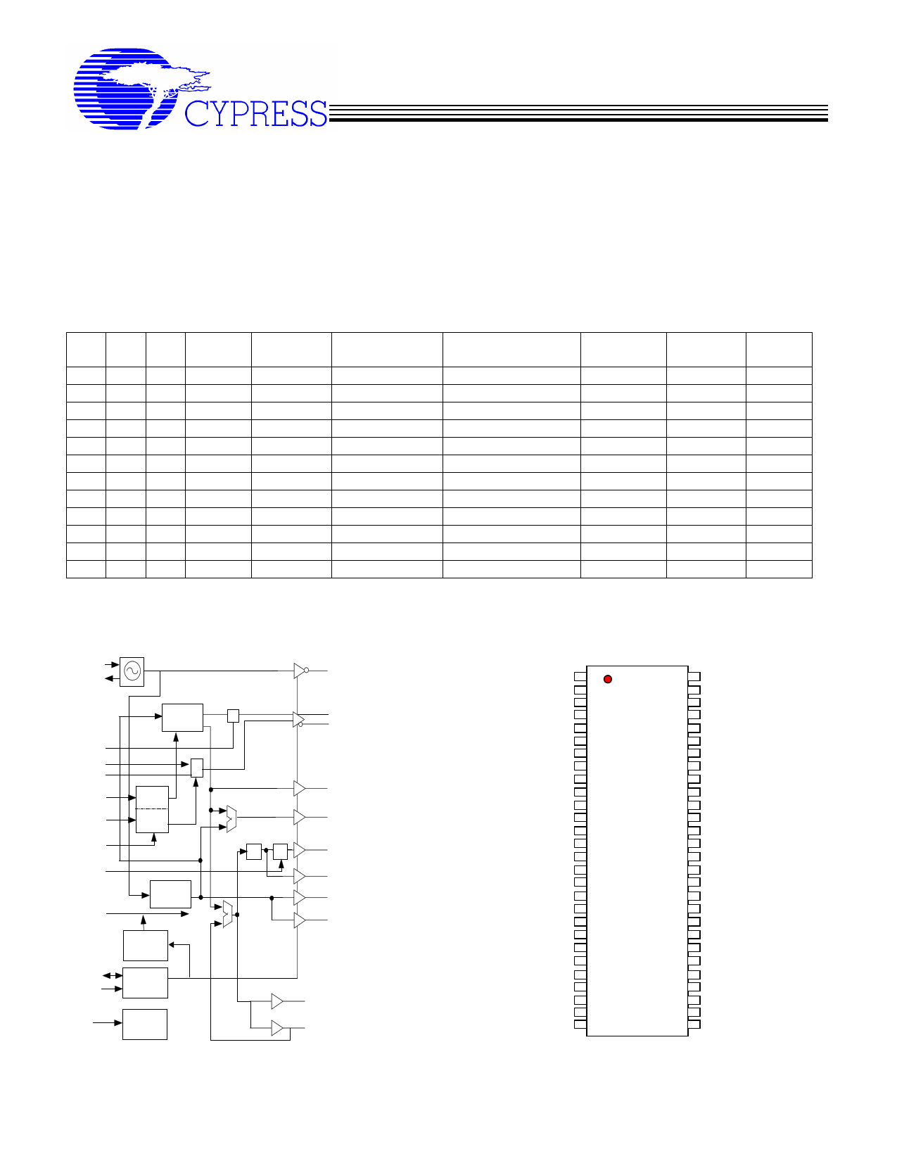
Block Diagram
XIN
XOUT
PLL1
CPU_STP#
IREF
VSSIREF
S(0:2)
MULT0
VTT_PG#
PCI_STP#
PD#
SDATA
SCLK
VDDA
PLL2
WD
Logic
I2C
Logic
Power
Up Logic
REF
CPU(0:2)
CPU/(0:2)
3V66_0
3V66_1/VCH
/2 PCI(0:6)
PCI_F(0:2)
48M USB
48M DOT
66B[0:2]/3V66[2:4]
66IN/3V66-5
Pin Configuration
VDD
XIN
XOUT
VSS
PCIF0
PCIF1
PCIF2
VDD
VSS
PCI0
PCI1
PCI2
PCI3
VDD
VSS
PCI4
PCI5
PCI6
VDD
VSS
66B0/3V66_2
66B1/3V66_3
66B2/3V66_4
66IN/3V66_5
PD#
VDDA
VSSA
VTT_PG#
1
2
3
4
5
6
7
8
9
10
11
12
13
14
15
16
17
18
19
20
21
22
23
24
25
26
27
28
56 REF
55 S1
54 S0
53 CPU_STP#
52 CPU0
51 CPU/0
50 VDD
49 CPU1
48 CPU/1
47 VSS
46 VDD
45 CPU2
44 CPU/2
43 MULT0
42 IREF
41 VSSIREF
40 S2
39 48MUSB
38 48MDOT
37 VDD
36 VSS
35 3V66_1/VCH
34 PCI_STP#
33 3V66_0
32 VDD
31 VSS
30 SCLK
29 SDATA
Cypress Semiconductor Corporation
http://www.cypress.com
Document#: 38-07108 Rev. *A
12/26/2002
Page 1 of 25
1 page 
Approved Product
C9870G
High Performance Pentium® 4 Clock Synthesizer
Byte 4: DRCG Control Register
(all bits are read and write functional)
Bit @Pup Pin# Description
70
- SS2 Spread Spectrum control bit
(0=down spread, 1=Center spread)
60
- Reserved
5 1 33 3V66_0 Output Enabled
1 = enabled, 0 = disabled
4 1 35 3V66_1/VCH Output Enable
1 = enabled, 0 = disabled
3 1 24 3V66_5 Output Enable
1 = enabled, 0 = disabled
2 1 23 66B2/3V66_4 Output Enabled
1 = enabled, 0 = disabled
1 1 22 66B1/3V66_3 Output Enabled
1 = enabled, 0 = disabled
0 1 21 66B0/3V66_2 Output Enabled
1 = enabled, 0 = disabled
Byte 6: Silicon Signature Register
(all bits are read only)
Bit @Pup Pin# Description
70
-
60
50
- Vendor Code
- 011 = IMI
40
-
30
-
20
-
11
-
01
-
Note: When writing to this register the device will acknowledge the
write operation, but the data itself will be ignored.
Byte 8: Dial-a-Frequency™ Control Register N
(all bits are read and write functional)
Bit @Pup Pin# Description
70
0 N7, MSB
60
0 N6
50
0 N5
40
0 N4
30
0 N3
20
0 N2
10
0 N3
00
0 N0, LSB
66IN to 66M Delay Control Table
Byte5
Bit5 Bit4
00
01
10
11
Delay (ns)
4.29
4.43
3.95 (default)
3.95
Byte 5: Clock control register
(all bits are read and write functional)
Bit @Pup Pin# Description
70
- SS1 Spread Spectrum control bit
61
- SS0 Spread Spectrum control bit
50
- 66IN to 66M delay Control MSB, See table
40
- 66IN to 66M delay Control LSB, See table
30
- Reserved
20
- 48MDOT edge rate control. When set to 1,
the edge is slowed by 15%.
10
- Reserved
00
- USB edge rate control. When set to 1, the
edge is slowed by 15%
Byte 7: Watch Dog Time Stamp Register
Bit @Pup Pin# Description
70
- Reserved
60
- Reserved
50
- Reserved
40
- Reserved
30
- Reserved
20
- Reserved
10
- Reserved
00
- Reserved
Byte 9: Dial-a-Frequency™ Control Register R
(all bits are read and write functional)
Bit @Pup Pin# Description
70
- R6 MSB
60
- R5
50
- R4
40
- R3
30
- R2
20
- R1
10
- R0, LSB
00
- R and N register load gate 0=gate closed
(data is latched), 1=gate open (data is
loading from SMBus registers into R and
N)
Cypress Semiconductor Corporation
http://www.cypress.com
Document#: 38-07108 Rev. *A
12/26/2002
Page 5 of 25
5 Page 
Approved Product
C9870G
High Performance Pentium® 4 Clock Synthesizer
Test and Measurement Setup (Cont.)
For single Ended Output Signals
3.3V signals
tDC
-
3.3V
Output under Test
Probe
Load Cap
-
2.4V
1.5V
0.4V
Tr
0V
Tf
Buffer Characteristics
Current Mode CPU Clock Buffer Characteristics
The current mode output buffer detail and current reference circuit details are contained in the previous table of this
data sheet. The following parameters are used to specify output buffer characteristics:
1. Output impedance of the current mode buffer circuit - Ro (see figure below).
2. Minimum and maximum required voltage operation range of the circuit – Vop (see figure below).
3. Series resistance in the buffer circuit – Ros (see figure below).
4. Current accuracy at given configuration into nominal test load for given configuration.
Cypress Semiconductor Corporation
http://www.cypress.com
Document#: 38-07108 Rev. *A
12/26/2002
Page 11 of 25
11 Page | ||
| Páginas | Total 25 Páginas | |
| PDF Descargar | [ Datasheet C9870G.PDF ] | |
Hoja de datos destacado
| Número de pieza | Descripción | Fabricantes |
| C9870G | Clock Synthesizer | Cypress Semiconductor |
| Número de pieza | Descripción | Fabricantes |
| SLA6805M | High Voltage 3 phase Motor Driver IC. |
Sanken |
| SDC1742 | 12- and 14-Bit Hybrid Synchro / Resolver-to-Digital Converters. |
Analog Devices |
|
DataSheet.es es una pagina web que funciona como un repositorio de manuales o hoja de datos de muchos de los productos más populares, |
| DataSheet.es | 2020 | Privacy Policy | Contacto | Buscar |