|
|
|
PDF BTS7750GP Data sheet ( Hoja de datos )
| Número de pieza | BTS7750GP | |
| Descripción | TrilithIC | |
| Fabricantes | Infineon Technologies | |
| Logotipo | ||
Hay una vista previa y un enlace de descarga de BTS7750GP (archivo pdf) en la parte inferior de esta página. Total 16 Páginas | ||
|
No Preview Available !
www.DataSheet4U.com
TrilithIC
BTS 7750 GP
Data Sheet
1 Overview
1.1 Features
• Quad D-MOS switch driver
• Free configurable as bridge or quad-switch
• Optimized for DC motor management applications
• Low RDS ON: 70 mτ high-side switch, 45 mτ low-
side switch (typical values @ 25 C)
• Maximum peak current: typ. 12 A @ 25 C=
• Very low quiescent current: typ. 5 ←A @ 25 C=
• Small outline, thermal optimized PowerPak
• Full short-circuit-protection
• Operates up to 40 V
• Status flag diagnosis
• Overtemperature shut down with hysteresis
• Internal clamp diodes
• Isolated sources for external current sensing
• Under-voltage detection with hysteresis
• PWM frequencies up to 1 kHz
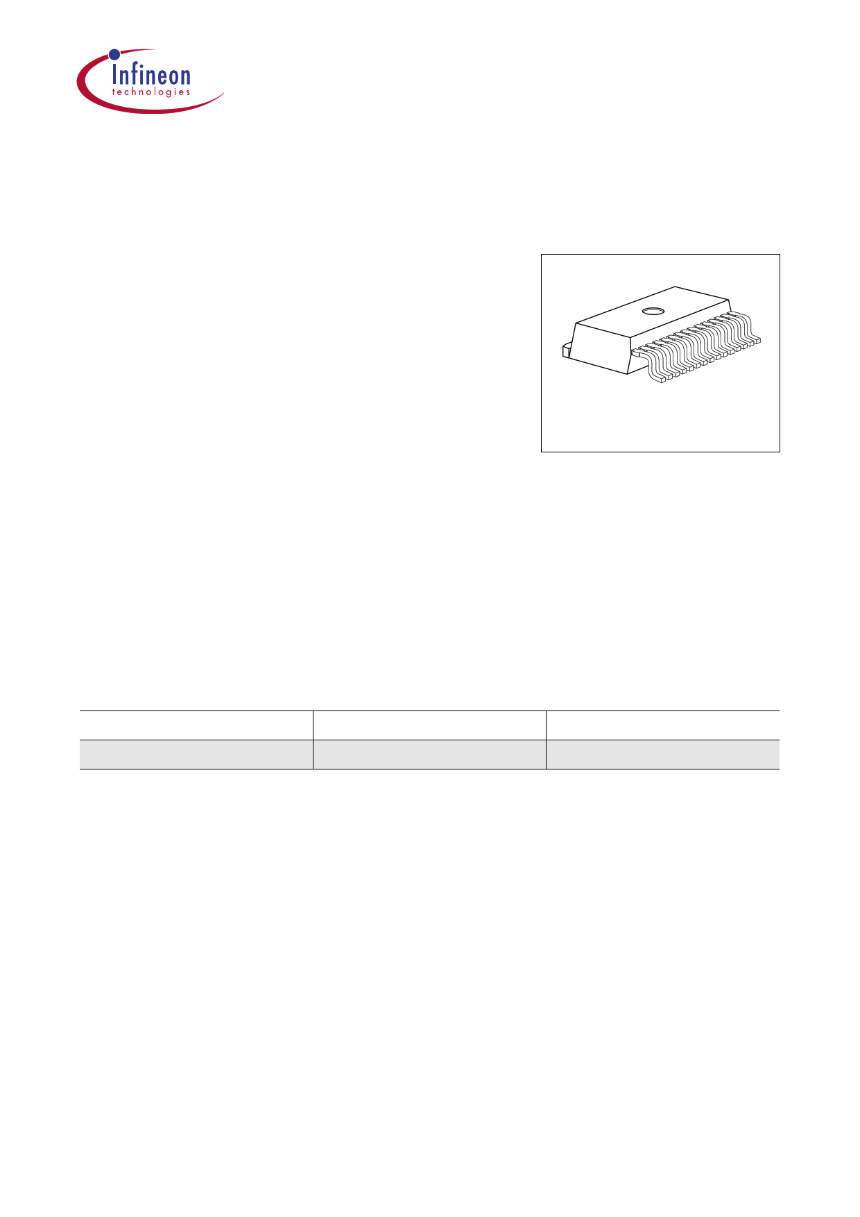
P-TO263-15-1
Type
BTS 7750 GP
Ordering Code
Q67006-A9402
Package
P-TO263-15-1
1.2 Description
The BTS 7750 GP is part of the TrilithIC family containing three dies in one package:
One double high-side switch and two low-side switches. The drains of these three
vertical DMOS chips are mounted on separated leadframes. The sources are connected
to individual pins, so the BTS 7750 GP can be used in H-bridge- as well as in any other
configuration. Both the double high-side and the two low-side switches of the
BTS 7750 GP are manufactured in SMART SIPMOS® technology which combines low
RDS ON vertical DMOS power stages with CMOS control circuitry. The high-side switch is
fully protected and contains the control and diagnosis circuitry. Also the low-side
switches are fully protected, the equivalent standard product is the BTS 134 D.
In contrast to the BTS 7750 G, which consists of the same chips in an P-DSO-28
package, the P-TO263-15-1 PowerPack offers a much lower thermal resistance, which
opens up applications with even higher currents in the automotive and industrial area.
Data Sheet 1 2001-02-01
1 page 
BTS 7750 GP
1.6 Circuit Description
Input Circuit
The control inputs IH1,2 consist of TTL/CMOS compatible Schmitt-Triggers with
hysteresis. Buffer amplifiers are driven by these stages and convert the logic signal into
the necessary form for driving the power output stages. The inputs are protected by ESD
clamp-diodes.
The inputs IL1 and IL2 are connected to the internal gate-driving units of the N-channel
vertical power-MOS-FETs.
Output Stages
The output stages consist of an low RDS ON Power-MOS H-bridge. In H-bridge
configuration, the D-MOS body diodes can be used for freewheeling when commutating
inductive loads. If the high-side switches are used as single switches, positive and
negative voltage spikes which occur when driving inductive loads are limited by
integrated power clamp diodes.
Short Circuit Protection
The outputs are protected against
– output short circuit to ground
– output short circuit to the supply voltage, and
– overload (load short circuit).
An internal OP-Amp controls the Drain-Source-Voltage by comparing the DS-Voltage-
Drop with an internal reference voltage. Above this trippoint the OP-Amp reduces the
output current depending on the junction temperature and the drop voltage.
In the case of overloaded high-side switches the status output is set to low.
The fully protected low-side switches have no status output.
Overtemperature Protection
The high-side and the low-side switches also incorporate an overtemperature protection
circuit with hysteresis which switches off the output transistors. In the case of the high-
side switches, the status output is set to low.
Undervoltage-Lockout (UVLO)
When VS reaches the switch-on voltage VUVON the IC becomes active with a hysteresis.
The High-Side output transistors are switched off if the supply voltage VS drops below
the switch off value VUVOFF.
Data Sheet 5 2001-02-01
5 Page 
BTS 7750 GP
3.3 Electrical Characteristics (cont’d)
ISH1 = ISH2 = ISL1 = ISL2 = 0 A; – 40 C < Tj < 150 C; 8 V < VS < 18 V
unless otherwise specified
Parameter
Symbol Limit Values Unit Test Condition
min. typ. max.
Thermal Shutdown
Thermal shutdown junction
temperature
Thermal switch-on junction
temperature
Temperature hysteresis
Tj SD
Tj SO
αT
155 180 190 C –
150 170 180 C –
– 10 – C αT = TjSD – TjSO
Status Flag Output ST of highside switch
Low output voltage
Leakage current
Zener-limit-voltage
VST L
IST LK
VST Z
– 0.2 0.6 V IST = 1.6 mA
– – 10 ←A VST = 5 V
5.4 – V IST = 1.6 mA
Switching times of highside switch
Turn-ON-time;
to 90% VSH
tON
Turn-OFF-time;
to 10% VSH
tOFF
Slew rate on 10 to 30% VSH dV/dtON
–
–
–
85
80
–
Slew rate off 70 to 40% VSH -dV/
dtOFF
–
–
Note: switching times are guaranteed by design
180 ←s
RLoad = 12 τ
VS = 12 V
180 ←s
RLoad = 12 τ
VS = 12 V
1.1 V/←s RLoad = 12 τ
VS = 12 V
1.5 V/←s RLoad = 12 τ
VS = 12 V
Data Sheet 11 2001-02-01
11 Page | ||
| Páginas | Total 16 Páginas | |
| PDF Descargar | [ Datasheet BTS7750GP.PDF ] | |
Hoja de datos destacado
| Número de pieza | Descripción | Fabricantes |
| BTS7750G | TrilithIC | Infineon Technologies |
| BTS7750GP | TrilithIC | Infineon Technologies |
| Número de pieza | Descripción | Fabricantes |
| SLA6805M | High Voltage 3 phase Motor Driver IC. |
Sanken |
| SDC1742 | 12- and 14-Bit Hybrid Synchro / Resolver-to-Digital Converters. |
Analog Devices |
|
DataSheet.es es una pagina web que funciona como un repositorio de manuales o hoja de datos de muchos de los productos más populares, |
| DataSheet.es | 2020 | Privacy Policy | Contacto | Buscar |