|
|
PDF LA7137M Data sheet ( Hoja de datos )
| Número de pieza | LA7137M | |
| Descripción | DVD Analog Video Outpit I/F IC | |
| Fabricantes | Sanyo Semicon Device | |
| Logotipo | ||
Hay una vista previa y un enlace de descarga de LA7137M (archivo pdf) en la parte inferior de esta página. Total 17 Páginas | ||
|
No Preview Available !
Ordering number : EN6206
www.DataSheet4U.com
LA7137M Monolithic Linear IC
DVD Analog Video Output I/F IC
Overview
The LA7137M is a video output interface IC for DVD players and is optimal as the driver IC for DVD players that provide
composite signal/S signal, component signal, and RGB signal video outputs.
Since this IC integrates a Y/C mixer on the same chip, the D/A converter composite output can be omitted. The LA7137M
also integrates S1 and S2 DC voltage and D/A converter reference voltage generation on chip, allowing most components
other than the drivers to be omitted.
Functions
• Clamps
• Amplifier
• 75Ω driver
• Y/C mixer
• S1 and S2 DC output
• D/A converter reference voltage output
Features
• Video signal-to-noise ratio : -80dB
• Frequency characteristics : flat to 10MHz
• Y/C time difference : less than 2ns
• Signal dynamic range : 170IRE.
• Can support all major signal types : composite/S signals, component signals, and baseband (RGB) signals. Furthermore,
the IC input type can be switched by the system microcontroller (since the input capacitors are shared).
• Two 75Ω driver systems that can be independently muted by the system microcontroller.
• The clamp pulses required for component signal input are generated internally in the IC.
• Either of two amplifier gain levels, 8.5 and 6dB, can be selected.
• A built-in regulator circuit provides a stable DC voltage output that is independent of VCC fluctuations.
Specifications
Maximum Ratings at Ta = 25°C
Parameter
Symbol
Conditions
Maximum supply voltage
Allowable power dissipation
VCC max
Pd max
Ta ≤ 75°C * Mounted on a board
Operating temperature
Topr
Storage temperature
Tstg
* Only when mounted on a 114.3×76.1×1.6mm3 glass epoxy board
Ratings
10.0
525
-20 to +75
-40 to +150
Unit
V
mW
°C
°C
Any and all SANYO Semiconductor products described or contained herein do not have specifications
that can handle applications that require extremely high levels of reliability, such as life-support systems,
aircraft's control systems, or other applications whose failure can be reasonably expected to result in
serious physical and/or material damage. Consult with your SANYO Semiconductor representative
nearest you before using any SANYO Semiconductor products described or contained herein in such
applications.
SANYO Semiconductor assumes no responsibility for equipment failures that result from using products
at values that exceed, even momentarily, rated values (such as maximum ratings, operating condition
ranges, or other parameters) listed in products specifications of any and all SANYO Semiconductor
products described or contained herein.
N1506 MS PC B8-4581 No.6206-1/17
1 page 
LA7137M
Continued from preceding page.
Symbol
VDC1
VDC2
Control voltage (unit: V)
VDC4
VDC5
VDC11
VDC22
(N) The gain ratios between the different signals when baseband is selected
∆B1
0/3.3
-
-
- 3.3 3.3
∆B2
0/3.3
-
-
- 3.3 3.3
∆B3
0/3.3
-
-
- 3.3 3.3
(O) Gain frequency characteristics (Common to all modes and input signals other than Y/C mixed mode)
FY6
0/3.3
0
-
FY10
0/3.3
0
-
(P) DC voltage when output muting applied (Common to all modes)
-
-
3.3 3.3
3.3 3.3
V13
0
-
-
-
0/3.3
0/3.3
V15
3.3 -
-
-
0/3.3
0/3.3
V17
0
-
-
-
0/3.3
0/3.3
V19
3.3 -
-
-
0/3.3
0/3.3
V21
0
-
-
-
0/3.3
0/3.3
V23
3.3 -
-
-
0/3.3
0/3.3
(Q) Output DC voltage characteristics
VDA
V43
VLB
VSQ
-
-
-
-
0/3.3
0/3.3
-
-
0
0
0/3.3
0/3.3
-
-
0
3.3
0/3.3
0/3.3
-
-
3.3
0
0/3.3
0/3.3
Switching conditions
SW1
SW2
ON/OFF
ON/OFF
ON/OFF
OFF
OFF
OFF
ON/OFF
ON/OFF
ON
ON
ON -
ON -
ON -
ON -
ON -
ON -
--
--
--
--
Control Pin Functions
Pin No.
Pin state
Low Open High
1
Pin voltage
0 to 0.6V
1.55 to 1.75V
2.7 to 5V
75Ω driver muting
13, 17, 21 muted
Not muted
15, 19, 23 muted
2
Pin voltage
0 to 0.6V
1.55 to 1.75V
2.7 to 5V
Signal input type switching
Composite/S mode
Baseband mode
Component mode
11 Pin voltage
0 to 1V
2.7 to 8V (note)
Amplifier gain switching
6dB
8.5dB
22 Pin voltage
0 to 1V
2.7 to 8V (note)
Y/C mixer control
Y/C mixed mode
Composite mode
Note : Never apply a voltage higher than the VCC voltage at pins 9 and 20 to pin 11 or pin 22.
* : Y/C mixed mode is illegal in modes other than composite/S mode.
* : In composite mode, use pin 6 to input the chrominance signal capacitor-coupled, pin 3 for the clamped composite
signal, and pin 10 for the clamped Y signal. However, in S mode, pin 3 will have no input.
In component mode, pins 3 and 6 will be pedestal clamped B-Y and R-Y signals, respectively, while pin 10 will be
the clamped Y signal input.
In baseband mode, pins 3, 6, and 10 are all clamped inputs, for the RGB signals, respectively.
Pins 11 and 22 must never be left open.
Pin 4
0 to 1V
0 to 1V
2.6 to 5V
2.6 to 5V
Pin 5
0 to 1V
2.6 to 5V
0 to 1V
2.6 to 5V
Pin 16 output DC
Low (0V) → 4 : 3 mode
Middle (2.5V) → Letterbox mode
High (5V) → Squeezed mode
Illegal values
No.6206-5/17
5 Page 
LA7137M
Continued from preceding page.
Pin
Pin I/O
No.
16 C-DC.OUT
O
Pin
voltage
4.7V
I/O
impedance
4.1Ω
Description
The LA7137M creates, and outputs
from this pin, a stabilized DC voltage
based on the control information input to
pins 4 and 5. This pin outputs a low level
(0V) for 4 : 3 mode, a middle level (2.2V)
for letterbox mode, and a high level (5V)
for squeeze mode. A 10kΩ resistor must
be inserted to superimpose the DC
voltage output from pin 17 on the
capacitor coupled chrominance output.
(See the application circuit diagram.)
11 AMP-SW
I 2.4V
9.0GΩ
Control pin that switches the amplifier
gain to match the amplitude of the input
signal. This pin's input level can be
switched between VCC and ground on
the printed circuit board even by a 3.3 to
5.0V power supply microcontroller. (See
the control pin functions table.)
VCC
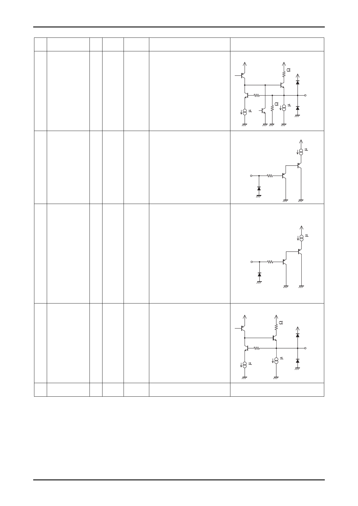
Equivalent circuit
VCC
VCC
200Ω
OUT
VCC
IN
5kΩ
22 COMPOSITE-
S.SW
12 DAC-DC.OUT
P 2.4V
O 3.4V
9.0GΩ
4.0Ω
Controls the on/off state of the Y/C
mixer. When using a D/A converter that
omits the composite output, the Y/C
mixer must be turned on. At the same
time as mixing the Y signal input to pin
10 with the chrominance signal input to
pin 6, pin 3 will be dropped to ground.
When pin 2 control specifies a signal
type other than composite/S signal, this
pin must be tied high. This pin's input
level can be switched between VCC
and ground on the printed circuit board
even by a 3.3 to 5.0V power supply
microcontroller. (See the control pin
functions table.)
Outputs a DC reference voltage for use
by a D/A converter. In particular, it
outputs a 3.3V level. This reference
voltage is unaffected by VCC
fluctuations or temperature and can be
used in conjunction with a resistor
divider to produce the DC level required
by the D/A converter.
VCC
IN
5kΩ
VCC
VCC
VCC
200Ω
OUT
7 GND1
P 0V
Ground for systems other than the 75Ω
driver system.
Continued on next page.
No.6206-11/17
11 Page | ||
| Páginas | Total 17 Páginas | |
| PDF Descargar | [ Datasheet LA7137M.PDF ] | |
Hoja de datos destacado
| Número de pieza | Descripción | Fabricantes |
| LA7137M | DVD Analog Video Outpit I/F IC | Sanyo Semicon Device |
| Número de pieza | Descripción | Fabricantes |
| SLA6805M | High Voltage 3 phase Motor Driver IC. |
Sanken |
| SDC1742 | 12- and 14-Bit Hybrid Synchro / Resolver-to-Digital Converters. |
Analog Devices |
|
DataSheet.es es una pagina web que funciona como un repositorio de manuales o hoja de datos de muchos de los productos más populares, |
| DataSheet.es | 2020 | Privacy Policy | Contacto | Buscar |
