|
|
|
PDF U4091BM Data sheet ( Hoja de datos )
| Número de pieza | U4091BM | |
| Descripción | Programmable Telephone Audio Processor | |
| Fabricantes | TEMIC Semiconductors | |
| Logotipo | ||
Hay una vista previa y un enlace de descarga de U4091BM (archivo pdf) en la parte inferior de esta página. Total 29 Páginas | ||
|
No Preview Available !
www.DataSheet4U.com
Programmable Telephone Audio Processor
U4091BM
Description
The programmable telephone audio processor U4091BM
is a linear integrated circuit for use in feature phones,
answering machines and fax machines. It contains the
speech circuit, tone-ringer interface with DC/DC
converter, sidetone equivalent and ear-protection
rectifiers. The circuit is line-powered and contains all
components necessary for signal amplification and
adaptation to the line. The U4091BM can also be supplied
via an external power supply. An integrated voice switch
with loudspeaker amplifier enables hands-free or
loudhearing operation. With an anti-feedback function,
acoustical feedback during loudhearing can be reduced
significantly. The generated supply voltage is suitable for
a wide range of peripheral circuits.
Features
D Speech circuit with anti-clipping
D Tone-ringer interface with DC/DC converter
D Speaker amplifier with anti-distortion
D Power-supply management (regulated, unregulated)
and a special supply for electret microphone
D Voice switch
D Interface for answering machine and cordless phone
Benefits
D No piezoelectric transducer for tone ringing necessary
D Complete system integration of analog signal proces-
sing on one chip
D Very few external components
Applications
Feature phone, answering machine, fax machine, speaker
phone, cordless phone
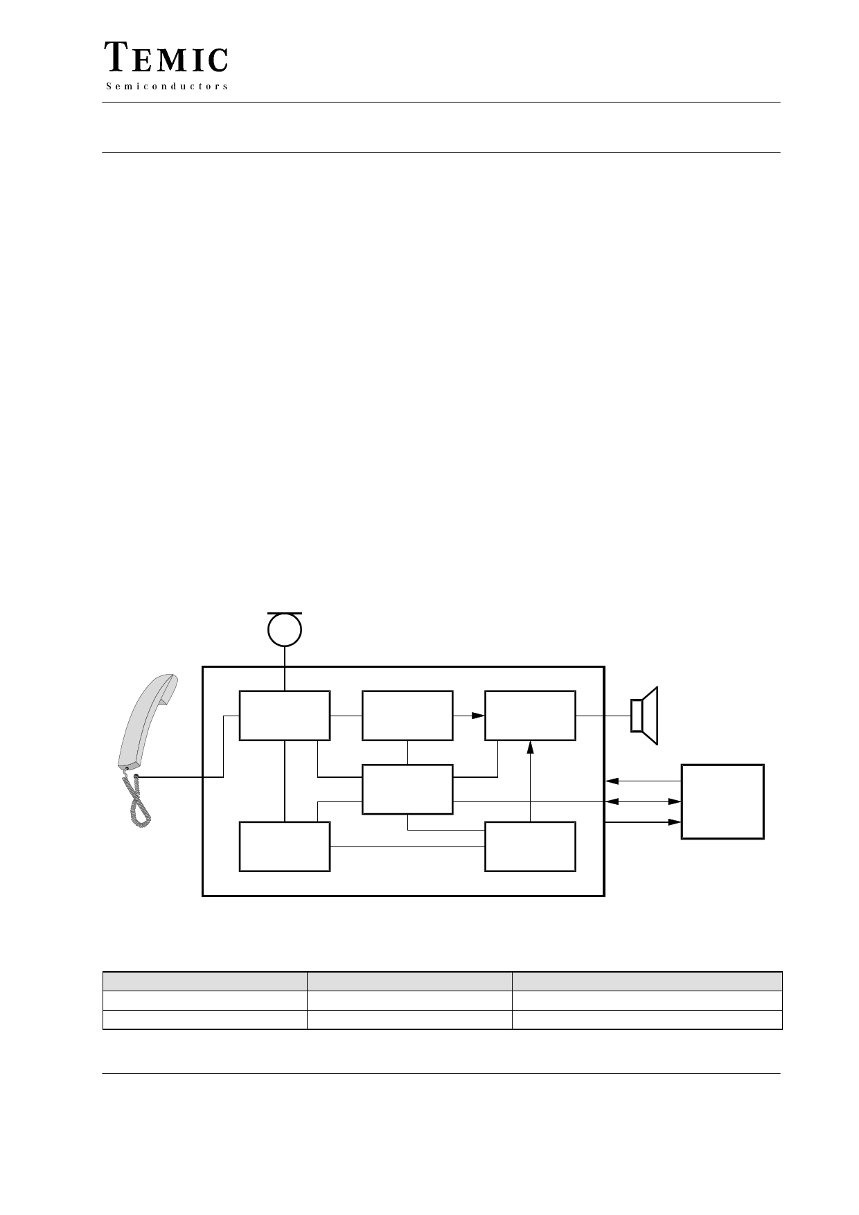
Block Diagram
Speech
circuit
DTMF
Ordering Information
Extended Type Number
U4091BM-AFN
U4091BM-AFNG3
Voice
switch
Serial
bus
Audio
amplifier
Tone
ringer
Clock
Data
Reset
MCU
14601
Package
SSO44
SSO44
Remarks
Taped and reeled
Rev. A1, 02-Jun-98
Target Specification
1 (29)
1 page 
U4091BM
For line voltages below 2 V, the switches remain in Ringing Frequency Detector (RFD)
quiescent state as shown in the diagram.
The U4091BM provides an output signal for the
2. When the chip is in power-down mode (Bit microcontroller. This output signal is always double the
LOMAKE), e.g., during pulse dialing, all internal value of the input signal (ringing frequency). It is
blocks are disabled via the serial bus. In this condition, generated by a current comparator with hysteresis. The
the voltage regulators and their internal bandgap are levels for the on-threshold are programmable in 16 steps;
the only active blocks.
the off-level is fixed. Every change of the comparator
output generates a high level at the interrupt output INT.
3. During ringing, the supply for the system is fed into The information can then be read out by means of a serial
VB via the Ringing Power Converter (RPC). bus with either normal or fast read mode. The block RFD
Normally, the speaker amplifier in single-ended mode is always enabled.
is used for ringing. The frequency for the melody is
generated by the DTMF/Melody generator.
ÁÁÁÁÁÁÁÁÁÁÁÁÁÁÁÁÁÁÁÁÁÁÁÁÁÁÁÁÁÁÁÁ4. In an answering machine, the chip is powered by an
ÁÁÁÁÁÁÁÁÁÁÁÁÁÁÁÁexternal supply via Pin VB. The answering machine
connections can be directly put to U4091BM. The
ÁÁÁÁÁÁÁÁÁÁÁÁÁÁÁÁanswering machine is connected to the Pin AMREC.
RINGTH[0:3]
0
15
VRING
7V
22 V
step 1 V
Clock Output Divider Adjustment
For the output AMREC, an AGC function is select-
able via the serial bus. The output of the answering
machine will be connected to the Pin AMPB, which is
directly connected to the switching matrix, and thus
enables the signal to be switched to every desired
output.
The Pin OSCOUT is a clock output which is derived from
the crystal oscillator. It can be used to drive a micro-
controller or another remote component and thereby
reduces the number of crystals required. The oscillator
frequency can be divided by 1, 8, 16, 32. During power-on
reset, the divider will be reset to 1 until it is changed by
setting the serial bus.
VL RSENSE
10 Ω
C
1 µF
IND
+
–
ÁÁÁÁÁÁÁÁÁÁÁÁÁÁÁÁ5.5 V
VMPS
ÁÁÁÁÁÁÁÁÁÁÁÁÁÁÁÁÁÁÁÁÁÁÁÁÁÁÁÁÁÁÁÁ470µF
ÁÁÁÁÁÁÁÁÁÁÁÁÁÁÁÁ–
CLK[0:1]
0
1
2
3
Divider
1
8
16
32
Frequency
3.58 MHz
447 kHz
224 kHz
112 kHz
+ 3.3 V VMP Serial Bus Interface
R
R
300 kΩ
V
+ 47 µF
–
5.5 V
VB
220µF
14573
Figure 3. Supply generator
Ringing Power Converter (RPC)
The circuit is controlled by an external microcontroller
through the serial bus.
The serial bus is a bi-directional system consisting of a
one-directional clock line (SCL) which is always driven
by the microcontroller, and a bi-directional data-signal
line. It is driven by the microcontroller as well as from the
U4091BM (see fig. 23).
The serial bus requires external pull-up resistors as only
pull-down transistors (Pin SDA) are integrated.
WRITE: The data is a 12-bit word:
The RPC transforms the input power at VRING (high
voltage/ low current) into an equivalent output power at
VB (low voltage/ high current) which is capable of
driving the low-ohmic loudspeaker. The input impedance
at VRING is adjustable from 3 kW to 12 kW by RIMPA
(ZRING = RIMPA / 100) and the efficiency of the step-
down converter is approximately 65%.
A0 – A3: address of the destination register (0 to 15)
D0 – D7: content of the register
The data line must be stable when the clock is high. Data
must be shifted serially.
After 12 clock periods, the write indication is sent. Then,
the transfer to the destination register is (internally)
generated by a strobe signal transition of the data line
when the clock is high.
Rev. A1, 02-Jun-98
Target Specification
5 (29)
5 Page 
U4091BM
Acoustic Feedback Suppression
Acoustical feedback from the loudspeaker to the hands-
free microphone may cause instability of the system. The
U4091BM has a very efficient feedback-suppression
circuit which offers a 4-point- or alternatively a 2-point-
signal-sensing topology (see figure 7).
Two attenuators (TXA and SAI) reduce the critical loop
gain via the serial bus either in the transmit or in the
receive path. The overall loop gain remains constant
under all operating conditions.
The LOGs produce a logarithmically-compressed signal
of the TX- and RX-envelope curve. The block AFSCON
determines whether the TX or the RX signal has to be
attenuated.
The voice-switch topology can be selected by the serial
bus. In 2-point-sensing mode, AFSCON is controlled
directly by the LOG outputs.
MICRO
MICO
TXA
CTU
RTU
INLDT
CTLO CBNMT
TLDT BNMT
LOG
AGATX
LOG
CALCT
STO
BNM
Mode
control
BNM
Line
LOG
CALCR
AFSCON
AGARX
LOG
CT BNMR TLDR
INLDR
RRU
CCT CBNMR CRLO
CRU
RECO1
HV
SA DTD
SAI
RECO2
14577
Figure 7. Basic system configurations.
Rev. A1, 02-Jun-98
Target Specification
11 (29)
11 Page | ||
| Páginas | Total 29 Páginas | |
| PDF Descargar | [ Datasheet U4091BM.PDF ] | |
Hoja de datos destacado
| Número de pieza | Descripción | Fabricantes |
| U4091B | Programmable Telephone Audio Processor | TEMIC Semiconductors |
| U4091BM | Programmable Telephone Audio Processor | TEMIC Semiconductors |
| U4091BM-N | Programmable Telephone Audio Processor | ATMEL Corporation |
| Número de pieza | Descripción | Fabricantes |
| SLA6805M | High Voltage 3 phase Motor Driver IC. |
Sanken |
| SDC1742 | 12- and 14-Bit Hybrid Synchro / Resolver-to-Digital Converters. |
Analog Devices |
|
DataSheet.es es una pagina web que funciona como un repositorio de manuales o hoja de datos de muchos de los productos más populares, |
| DataSheet.es | 2020 | Privacy Policy | Contacto | Buscar |