|
|
|
PDF CS5203-1 Data sheet ( Hoja de datos )
| Número de pieza | CS5203-1 | |
| Descripción | 3.0 A Adjustable Linear Regulator | |
| Fabricantes | ON Semiconductor | |
| Logotipo | ||
Hay una vista previa y un enlace de descarga de CS5203-1 (archivo pdf) en la parte inferior de esta página. Total 10 Páginas | ||
|
No Preview Available !
www.DataSheet4U.com
CS5203−1
3.0 A Adjustable Linear
Regulator
The CS5203−1 linear regulator provides 3.0 A at adjustable output
voltages with an accuracy of ±1.5 %. The device uses two external
resistors to set the output voltage within a 1.25 V to 5.5 V range.
The regulator is intended for use as a post regulator and
microprocessor supply. The fast loop response and low dropout
voltage make this regulator ideal for applications where low voltage
operation and good transient response are important.
The circuit is designed to operate with dropout voltages less than 1.4 V
at 3.0 A output current. Device protection includes overcurrent and
thermal shutdown.
The CS5203−1 is pin compatible with the LT1085 family of linear
regulators but has lower dropout voltage.
The regulator is available in TO−220−3 and surface mount D2PAK−3
packages.
Features
• Output Current to 3.0 A
• Output Accuracy to ±1.5% Over Temperature
• Dropout Voltage (typical) 1.2 V @ 3.0 A
• Fast Transient Response
• Fault Protection
− Current Limit
− Thermal Shutdown
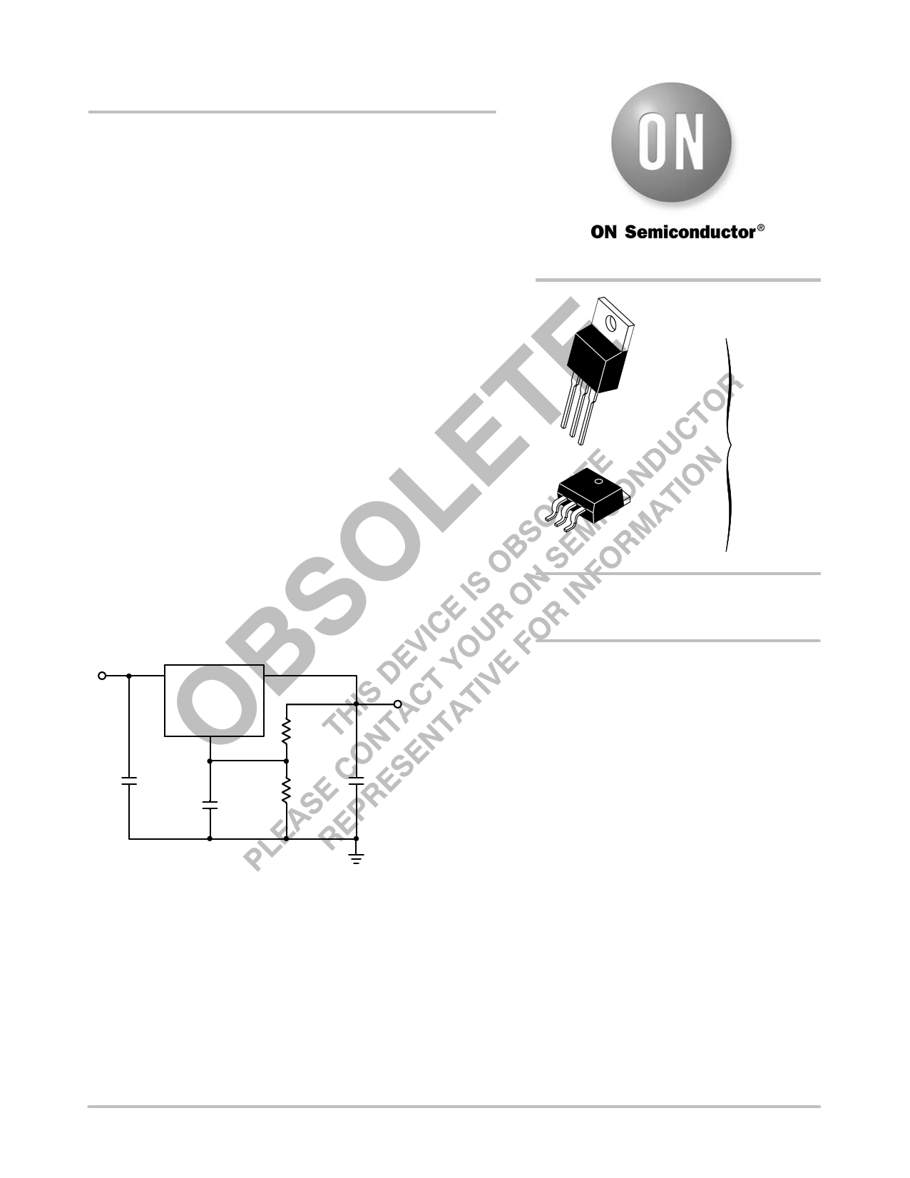
5.0 V
VIN VOUT
CS5203−1
Adj
10 mF
5.0 V
0.1 mF
5.0 V
124 W
1.0%
200 W
1.0%
3.3 V @ 3.0 A
22 mF
5.0 V
http://onsemi.com
12 3
123
TO−220−3
T SUFFIX
CASE 221A
D2PAK−3
DP SUFFIX
CASE 418AB
Tab = VOUT
Pin 1. Adj
2. VOUT
3. VIN
ORDERING INFORMATION
See detailed ordering and shipping information in the package
dimensions section on page 8 of this data sheet.
DEVICE MARKING INFORMATION
See general marking information in the device marking
section on page 8 of this data sheet.
Figure 1. Applications Diagram
© Semiconductor Components Industries, LLC, 2006
September, 2006 − Rev. 8
1
Publication Order Number:
CS5203−1/D
1 page 
CS5203−1
APPLICATIONS INFORMATION
The CS5203−1 linear regulator provides adjustable voltages
at currents up to 3.0 A. The regulator is protected against
overcurrent conditions and includes thermal shutdown.
The CS5203−1 has a composite PNP−NPN output
transistor and requires an output capacitor for stability. A
detailed procedure for selecting this capacitor is included in
the Stability Considerations section.
Adjustable Operation
The CS5203−1 has an output voltage range of 1.25 V to
5.5 V. An external resistor divider sets the output voltage as
shown in Figure 12. The regulator maintains a fixed 1.25V
(typical) reference between the output pin and the adjust pin.
A resistor divider network R1 and R2 causes a fixed current
to flow to ground. This current creates a voltage across R2
that adds to the 1.25 V across R1 and sets the overall output
voltage. The adjust pin current (typically 50 mA) also flows
through R2 and adds a small error that should be taken into
account if precise adjustment of VOUT is necessary.
The output voltage is set according to the formula:
ǒ ǓVOUT + VREF
R1 ) R2
R1
) IAdj
R2
The term IAdj × R2 represents the error added by the adjust
pin current.
R1 is chosen so that the minimum load current is at least
2.0 mA. R1 and R2 should be the same type, e.g. metal film
for best tracking over temperature. While not required, a
bypass capacitor from the adjust pin to ground will improve
ripple rejection and transient response. A 0.1 mF tantalum
capacitor is recommended for “first cut” design. Type and
value may be varied to obtain optimum performance vs.
price.
In most applications, ramp−up of the power supply to VIN
is fairly slow, typically on the order of several tens of
milliseconds, while the regulator responds in less than one
microsecond. In this case, the linear regulator begins
charging the load as soon as the VIN to VOUT differential is
large enough that the pass transistor conducts current. The
load at this point is essentially at ground, and the supply
voltage is on the order of several hundred millivolts, with the
result that the pass transistor is in dropout. As the supply to
VIN increases, the pass transistor will remain in dropout, and
current is passed to the load until VOUT reaches the point at
which the IC is in regulation. Further increase in the supply
voltage brings the pass transistor out of dropout. The result
is that the output voltage follows the power supply ramp−up,
staying in dropout until the regulation point is reached. In
this manner, any output voltage may be regulated. There is
no theoretical limit to the regulated voltage as long as the
VIN to VOUT differential of 7.0 V is not exceeded.
However, the possibility of destroying the IC in a short
circuit condition is very real for this type of design. Short
circuit conditions will result in the immediate operation of
the pass transistor outside of its safe operating area.
Over−voltage stresses will then cause destruction of the pass
transistor before overcurrent or thermal shutdown circuitry
can become active. Additional circuitry may be required to
clamp the VIN to VOUT differential to less than 7.0 V if
fail−safe operation is required. One possible clamp circuit is
illustrated in Figure 13; however, the design of clamp
circuitry must be done on an application by application
basis. Care must be taken to ensure the clamp actually
protects the design. Components used in the clamp design
must be able to withstand the short circuit condition
indefinitely while protecting the IC.
VIN
VIN VOUT
VOUT
CS5203−1
C1
VREF
C2
Adj R1
EXTERNAL SUPPLY
IAdj
CAdj
R2
Figure 12. Resistor Divider Scheme
The CS5201−1 linear regulator has an absolute maximum
specification of 7.0 V for the voltage difference between VIN
and VOUT. However, the IC may be used to regulate voltages
in excess of 7.0 V. The main considerations in such a design
are power−up and short circuit capability.
VIN VOUT
VAdj
VOUT
Figure 13. Short Circuit Protection Circuit for
High Voltage Application.
http://onsemi.com
5
5 Page | ||
| Páginas | Total 10 Páginas | |
| PDF Descargar | [ Datasheet CS5203-1.PDF ] | |
Hoja de datos destacado
| Número de pieza | Descripción | Fabricantes |
| CS5203-1 | 3A Adjustable Linear Regulator | Cherry Semiconductor Corporation |
| CS5203-1 | 3.0 A Adjustable Linear Regulator | ON Semiconductor |
| CS5203-1GDP3 | 3A Adjustable Linear Regulator | Cherry Semiconductor Corporation |
| CS5203-1GDPR3 | 3A Adjustable Linear Regulator | Cherry Semiconductor Corporation |
| Número de pieza | Descripción | Fabricantes |
| SLA6805M | High Voltage 3 phase Motor Driver IC. |
Sanken |
| SDC1742 | 12- and 14-Bit Hybrid Synchro / Resolver-to-Digital Converters. |
Analog Devices |
|
DataSheet.es es una pagina web que funciona como un repositorio de manuales o hoja de datos de muchos de los productos más populares, |
| DataSheet.es | 2020 | Privacy Policy | Contacto | Buscar |