|
|
|
PDF NB2309A Data sheet ( Hoja de datos )
| Número de pieza | NB2309A | |
| Descripción | 3.3 V Zero Delay Clock Buffer | |
| Fabricantes | ON Semiconductor | |
| Logotipo | ||
Hay una vista previa y un enlace de descarga de NB2309A (archivo pdf) en la parte inferior de esta página. Total 9 Páginas | ||
|
No Preview Available !
NB2309A
3.3 V Zero Delay
Clock Buffer
The NB2309A is a versatile, 3.3 V zero delay buffer designed to
distribute high−speed clocks. It accepts one reference input and drives
out nine low−skew clocks. It is available in a 16 pin package.
The −1H version of the NB2309A operates at up to 133 MHz, and
has higher drive than the −1 devices. All parts have on−chip PLL’s that
lock to an input clock on the REF pin. The PLL feedback is on−chip
and is obtained from the CLKOUT pad.
The NB2309A has two banks of four outputs each, which can be
controlled by the Select inputs as shown in the Select Input Decoding
Table. If all the output clocks are not required, Bank B can be
three−stated. The select inputs also allow the input clock to be directly
applied to the outputs for chip and system testing purposes.
Multiple NB2309A devices can accept the same input clock and
distribute it. In this case the skew between the outputs of the two
devices is guaranteed to be less than 700 ps.
All outputs have less than 200 ps of cycle−to−cycle jitter. The input
and output propagation delay is guaranteed to be less than 350 ps, and
the output to output skew is guaranteed to be less than 250 ps.
The NB2309A is available in two different configurations, as shown
in the ordering information table. The NB2309A1 is the base part. The
NB2309Ax1H* is the high drive version of the −1 and its rise and fall
times are much faster than −1 part.
www.DataSheet4U.com
Features
• 15 MHz to 133 MHz Operating Range, Compatible with CPU and
PCI Bus Frequencies
• Zero Input − Output Propagation Delay
• Multiple Low−Skew Outputs
• Output−Output Skew Less than 250 ps
• Device−Device Skew Less than 700 ps
• One Input Drives 9 Outputs, Grouped as 4 + 4 + 1
• Less than 200 ps Cycle−to−Cycle Jitter is Compatible with PentiumR
Based Systems
• Test Mode to Bypass PLL
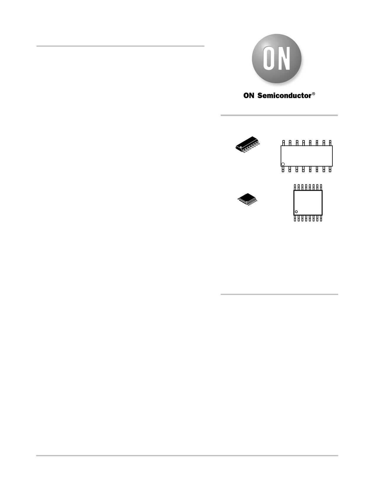
• Available in 16 Pin, 150 mil SOIC and 4.4 mm TSSOP
• 3.3 V Operation, Advanced 0.35 m CMOS Technology
• These are Pb−Free Devices**
http://onsemi.com
MARKING
DIAGRAMS*
16
1
SOIC−16
D SUFFIX
CASE 751B
16
1
TSSOP−16
DT SUFFIX
CASE 948F
16
XXXXXXXXG
AWLYWW
1
16
XXXX
XXXX
ALYWG
G
1
XXXX = Device Code
A = Assembly Location
WL, L = Wafer Lot
Y = Year
W, WW = Work Week
G or G = Pb−Free Package
*For additional marking information, refer to
Application Note AND8002/D.
ORDERING INFORMATION
See detailed ordering and shipping information in the package
dimensions section on page 7 of this data sheet.
*x = C for Commercial; I for Industrial.
**For additional information on our Pb−Free strategy and soldering details,
please download the ON Semiconductor Soldering and Mounting Techniques
Reference Manual, SOLDERRM/D.
© Semiconductor Components Industries, LLC, 2006
November, 2006 − Rev. 4
1
Publication Order Number:
NB2309A/D
1 page 
NB2309A
Table 6. SWITCHING CHARACTERISTICS (Commercial and Industrial) (Note 6)
Parameter
1/t1
Description
Output Frequency
1/t1 Duty Cycle = (t2 / t1) * 100
(−1, −1H)
(−1H)
Test Conditions
30 pF load
10 pF load
Measured at 1.4 V, FOUT = 66.67 MHz
< 50 MHz
t3 Output Rise Time (−1, −1H) Measured between 0.8 V and 2.0 V
(−1H)
t4 Output Fall Time
Measured between 2.0 V and 0.8 V
t5 Output−to−Output Skew
All outputs equally loaded
t6
Delay, REF Rising Edge to CLKOUT
Measured at VDD/2
Rising Edge
t7 Device−to−Device Skew
Measured at VDD/2 on the CLKOUT pins of
the device
t8 Output Slew Rate
Measured between 0.8 V and 2.0 V using
Test Circuit #2
tJ
tLOCK
Cycle−to−Cycle Jitter
PLL Lock Time
Measured at 66.67 MHz, loaded outputs
Stable power supply, valid clock presented
on REF pin
trin REF Input Rise Time
Measured between 0.8 V to 2.0 V
tfin REF Input Rise Fall Time
Measured between 2.0 V to 0.8 V
6. All parameters specified with loaded outputs and apply to both PLL−Mode and PLL−Bypass Mode.
Min Typ Max Unit
15 100 MHz
15 133.33
40 50 60 %
45 50
55
2.5 ns
1.5
1.5 ns
250 ps
0 ±350 ps
0 700 ps
1 V/ns
200 ps
1.0 ms
1.0 ns
1.0 ns
http://onsemi.com
5
5 Page | ||
| Páginas | Total 9 Páginas | |
| PDF Descargar | [ Datasheet NB2309A.PDF ] | |
Hoja de datos destacado
| Número de pieza | Descripción | Fabricantes |
| NB2309A | 3.3 V Zero Delay Clock Buffer | ON Semiconductor |
| Número de pieza | Descripción | Fabricantes |
| SLA6805M | High Voltage 3 phase Motor Driver IC. |
Sanken |
| SDC1742 | 12- and 14-Bit Hybrid Synchro / Resolver-to-Digital Converters. |
Analog Devices |
|
DataSheet.es es una pagina web que funciona como un repositorio de manuales o hoja de datos de muchos de los productos más populares, |
| DataSheet.es | 2020 | Privacy Policy | Contacto | Buscar |