|
|
|
PDF AAT1149 Data sheet ( Hoja de datos )
| Número de pieza | AAT1149 | |
| Descripción | Step-Down Converter | |
| Fabricantes | AAT | |
| Logotipo | ||
Hay una vista previa y un enlace de descarga de AAT1149 (archivo pdf) en la parte inferior de esta página. Total 20 Páginas | ||
|
No Preview Available !
AAT1149
3MHz Fast Transient
400mA Step-Down Converter
General Description
Features
SwitchReg™
The AAT1149 SwitchReg is a 3.0MHz step-down
converter with an input voltage range of 2.7V to
5.5V and output voltage as low as 1.0V. It is opti-
mized to react quickly to load variations and oper-
ate with a tiny 0603 inductor that is only 1mm tall.
The AAT1149 output voltage is programmable via
external feedback resistors. It can deliver 400mA of
load current while maintaining a low 45μA no load
quiescent current. The 3.0MHz switching frequen-
cy minimizes the size of external components while
keeping switching losses low.
The AAT1149 maintains high efficiency throughout
the operating range, which is critical for portable
applications.
The AAT1149 is available in a Pb-free, space-saving
2.0x2.1mm SC70JW-8 package and is rated over
the -40°C to +85°C temperature range.
• Ultra-Small 0603 Inductor (Height = 1mm)
• VIN Range: 2.7V to 5.5V
• VOUT Adjustable from 1.0V to VIN
• 400mA Max Output Current
• Up to 98% Efficiency
• 45μA No Load Quiescent Current
• 3.0MHz Switching Frequency
• 70μs Soft Start
• Fast Load Transient
• Over-Temperature Protection
• Current Limit Protection
• 100% Duty Cycle Low-Dropout Operation
• <1μA Shutdown Current
• SC70JW-8 Package
• Temperature Range: -40°C to +85°C
Applications
•
•www.DataSheet4U.com
•
•
•
•
Cellular Phones
Digital Cameras
Handheld Instruments
Microprocessor / DSP Core / IO Power
PDAs and Handheld Computers
USB Devices
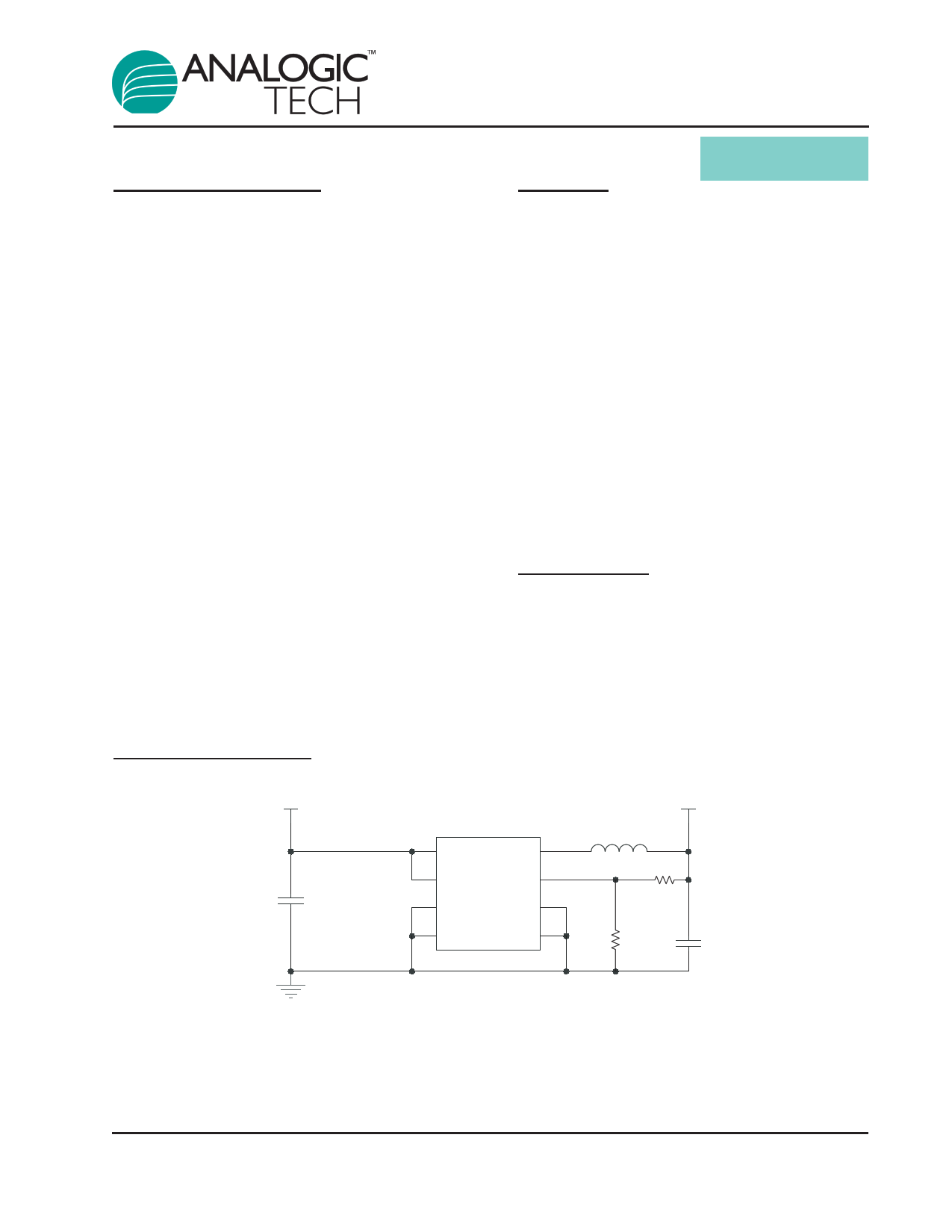
Typical Application
VIN = 3.6V
C2
4.7µF
U1
AAT1149
IN LX
EN FB
AGND PGND
PGND PGND
VOUT = 1.8V
L1 1.8µH
R1
118k
R2
59k
C1
4.7µF
1149.2006.11.1.0
1
1 page 
Typical Characteristics
Efficiency vs. Load Current
(VOUT = 3V; L = 3µH)
100
VIN = 3.3V
90
80
70 VIN = 4.2V VIN = 5V
60
50
0.1
1 10 100
Load Current (mA)
1000
Efficiency vs. Load Current
(VOUT = 1.8V; L = 2.2µH)
100
90 VIN = 3V
VIN = 3.6V
80
VIN = 2.7V
70 VIN = 5V
VIN = 4.2V
60
50
0.1
1 10 100
Load Current (mA)
1000
No Load Quiescent Current vs. Input Voltage
70
60 85°C
50
40
30 -40°C
20
10
0
2.5 3 3.5 4 4.5 5
Input Voltage (V)
25°C
5.5 6
AAT1149
3MHz Fast Transient
400mA Step-Down Converter
1.00
0.75
0.50
0.25
0.00
-0.25
-0.50
-0.75
-1.00
0.1
Load Regulation
(VOUT = 3V; L = 3µH)
VIN = 4.2V
VIN = 5V
VIN = 3.3V
1 10 100
Load Current (mA)
1000
Load Regulation
(VOUT = 1.8V; L = 2.2µH)
1.00
0.75
0.50
0.25
0.00
-0.25
-0.50
VIN = 5V
-0.75
-1.00
0.1
1
VIN = 3V
VIN = 4.2V
VIN = 3.6V
VIN = 2.7V
10 100 1000
Load Current (mA)
Switching Frequency vs. Input Voltage
2
1
VOUT = 1.1V
0
-1
-2
-3
VOUT = 1.8V
VOUT = 3V
-4
2.5 3 3.5 4 4.5 5
Input Voltage (V)
5.5
1149.2006.11.1.0
5
5 Page 
Control Loop
The AAT1149 is a peak current mode step-down
converter. The current through the P-channel
MOSFET (high side) is sensed for current loop
control, as well as short circuit and overload pro-
tection. A fixed slope compensation signal is added
to the sensed current to maintain stability for duty
cycles greater than 50%. The peak current mode
loop appears as a voltage-programmed current
source in parallel with the output capacitor.
The output of the voltage error amplifier programs
the current mode loop for the necessary peak
switch current to force a constant output voltage for
all load and line conditions. Internal loop compen-
sation terminates the transconductance voltage
error amplifier output. For the adjustable output,
the error amplifier reference is fixed at 0.6V.
Soft Start / Enable
Soft start limits the current surge seen at the input
and eliminates output voltage overshoot. When
pulled low, the enable input forces the AAT1149
into a low-power, non-switching state. The total
input current during shutdown is less than 1μA.
Current Limit and Over-Temperature
Protection
For overload conditions, the peak input current is
limited. To minimize power dissipation and stresses
under current limit and short-circuit conditions,
switching is terminated after entering current limit
for a series of pulses. Switching is terminated for
seven consecutive clock cycles after a current limit
has been sensed for a series of four consecutive
clock cycles.
Thermal protection completely disables switching
when internal dissipation becomes excessive. The
junction over-temperature threshold is 140°C with
15°C of hysteresis. Once an over-temperature or
over-current fault conditions is removed, the output
voltage automatically recovers.
Under-Voltage Lockout
Internal bias of all circuits is controlled via the IN
input. Under-voltage lockout (UVLO) guarantees
sufficient VIN bias and proper operation of all inter-
nal circuitry prior to activation.
1149.2006.11.1.0
AAT1149
3MHz Fast Transient
400mA Step-Down Converter
Applications Information
Inductor Selection
The step-down converter uses peak current mode
control with slope compensation to maintain stability
for duty cycles greater than 50%. The output induc-
tor value must be selected so the inductor current
down slope meets the internal slope compensation
requirements. Table 1 displays suggested inductor
values for various output voltages.
Manufacturer's specifications list both the inductor
DC current rating, which is a thermal limitation, and
the peak current rating, which is determined by the
saturation characteristics. The inductor should not
show any appreciable saturation under normal load
conditions. Some inductors may meet the peak and
average current ratings yet result in excessive loss-
es due to a high DCR. Always consider the losses
associated with the DCR and its effect on the total
converter efficiency when selecting an inductor.
The 1.8μH CDRH2D09 series inductor selected
from Sumida has a 131mΩ DCR and a 400mA sat-
uration current rating. At full load, the inductor DC
loss is 21mW which gives a 2.8% loss in efficiency
for a 400mA, 1.8V output.
Input Capacitor
Select a 4.7μF to 10μF X7R or X5R ceramic capac-
itor for the input. To estimate the required input
capacitor size, determine the acceptable input rip-
ple level (VPP) and solve for C. The calculated
value varies with input voltage and is a maximum
when VIN is double the output voltage.
VO · ⎛1 - VO ⎞
CIN =
VIN
⎛ VPP
⎝ IO
⎝ VIN ⎠
- ESR⎞⎠ · FS
VO
VIN
·
⎛⎝1 -
VO ⎞
VIN ⎠
=
1
4
for
VIN
=
2
·
VO
1
CIN(MIN) = ⎛ VPP
⎝ IO
- ESR⎞⎠ · 4 · FS
11
11 Page | ||
| Páginas | Total 20 Páginas | |
| PDF Descargar | [ Datasheet AAT1149.PDF ] | |
Hoja de datos destacado
| Número de pieza | Descripción | Fabricantes |
| AAT1140 | Fast Transient 600mA Step-Down Converter | Advanced Analog Technology |
| AAT1141 | Fast Transient 600mA Step-Down Converter | Advanced Analog Technology |
| AAT1142 | Voltage-Scaling Step-Down Converter | AAT |
| AAT1143 | 1MHz 400mA Step-Down Converter | Advanced Analogic Technologies |
| Número de pieza | Descripción | Fabricantes |
| SLA6805M | High Voltage 3 phase Motor Driver IC. |
Sanken |
| SDC1742 | 12- and 14-Bit Hybrid Synchro / Resolver-to-Digital Converters. |
Analog Devices |
|
DataSheet.es es una pagina web que funciona como un repositorio de manuales o hoja de datos de muchos de los productos más populares, |
| DataSheet.es | 2020 | Privacy Policy | Contacto | Buscar |