|
|
|
PDF LT1210 Data sheet ( Hoja de datos )
| Número de pieza | LT1210 | |
| Descripción | 1.1A/ 35MHz Current Feedback Amplifier | |
| Fabricantes | Linear Technology | |
| Logotipo | ||
Hay una vista previa y un enlace de descarga de LT1210 (archivo pdf) en la parte inferior de esta página. Total 16 Páginas | ||
|
No Preview Available !
LT1210
1.1A, 35MHz Current
Feedback Amplifier
FEATURES
s 1.1A Minimum Output Drive Current
s 35MHz Bandwidth, AV = 2, RL = 10Ω
s 900V/µs Slew Rate, AV = 2, RL = 10Ω
s High Input Impedance: 10MΩ
s Wide Supply Range: ±5V to ±15V
(TO-220 and DD Packages)
s Enhanced θJA SO-16 Package for ±5V Operation
s Shutdown Mode: IS < 200µA
s Adjustable Supply Current
s Stable with CL = 10,000pF
APPLICATIONS
s Cable Drivers
s Buffers
s Test Equipment Amplifiers
s Video Amplifiers
s ADSL Drivers
U
TYPICAL APPLICATIO S
DESCRIPTIO
The LT®1210 is a current feedback amplifier with high
output current and excellent large-signal characteristics.
The combination of high slew rate, 1.1A output drive and
±15V operation enables the device to deliver significant
power at frequencies in the 1MHz to 2MHz range. Short-
circuit protection and thermal shutdown ensure the
device’s ruggedness. The LT1210 is stable with large
capacitive loads, and can easily supply the large currents
required by the capacitive loading. A shutdown feature
switches the device into a high impedance and low
supply current mode, reducing dissipation when the
device is not in use. For lower bandwidth applications,
the supply current can be reduced with a single external
resistor.
The LT1210 is available in the TO-220 and DD packages
for operation with supplies up to ±15V. For ±5V applica-
tions the device is also available in a low thermal resis-
tance SO-16 package.
, LTC and LT are registered trademarks of Linear Technology Corporation.
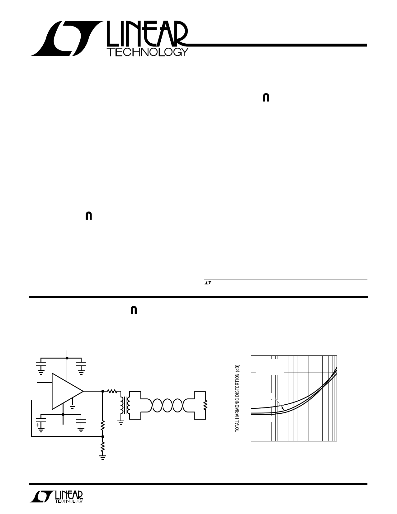
15V
+
4.7µF*
VIN +
LT1210
SD
–
+ 4.7µF*
–15V
Twisted Pair Driver
100nF
RT
11Ω
2.5W
T1**
13
RL
100Ω
2.5W
100nF
845Ω
274Ω
* TANTALUM
** MIDCOM 671-7783 OR EQUIVALENT
1210 TA01
Total Harmonic Distortion vs Frequency
–50
VS = ±15V
VOUT = 20VP-P
–60 AV = 4
–70
RL = 12.5Ω
–80 RL = 10Ω
RL = 50Ω
–90
–100
1k
10k 100k
FREQUENCY (Hz)
1M
1210 TA02
1
1 page 
WU
TYPICAL PERFOR A CE CHARACTERISTICS
LT1210
Bandwidth vs Supply Voltage
100
90
PEAKING ≤ 1dB
PEAKING ≤ 5dB
AV = 2
RL = 100Ω
80
70 RF = 470Ω
60 RF = 560Ω
50 RF = 750Ω
40 RF = 680Ω
30 RF = 1k
20
10 RF = 1.5k
0
4 6 8 10 12 14 16 18
SUPPLY VOLTAGE (±V)
1210 G01
Bandwidth vs Supply Voltage
100
90
PEAKING ≤ 1dB
PEAKING ≤ 5dB
AV = 10
RL = 100Ω
80
70
RF =390Ω
RF = 330Ω
60
50
RF = 470Ω
40
30 RF = 680Ω
20
10 RF = 1.5k
0
4 6 8 10 12 14 16 18
SUPPLY VOLTAGE (±V)
1210 G04
Differential Phase vs
Supply Voltage
0.6
0.5
RL = 10Ω
0.4 RF = RG = 750Ω
AV = 2
0.3 RL = 15Ω
0.2
0.1
0
5
RL = 50Ω
RL = 30Ω
7 9 11 13
SUPPLY VOLTAGE (±V)
15
1210 G07
Bandwidth vs Supply Voltage
50
PEAKING ≤ 1dB
PEAKING ≤ 5dB
40
AV = 2
RL = 10Ω
RF = 560Ω
30
RF = 750Ω
20 RF = 1k
10 RF = 2k
0
4 6 8 10 12 14 16 18
SUPPLY VOLTAGE (±V)
1210 G02
Bandwidth vs Supply Voltage
50
PEAKING ≤ 1dB
40
AV = 10
RL = 10Ω
Bandwidth and Feedback Resistance
vs Capacitive Load for Peaking ≤ 1dB
10k 100
BANDWIDTH
1k 10
FEEDBACK RESISTANCE
AV
RL
=
=
2
∞
VS = ±15V
CCOMP = 0.01µF
100
1 10
100
1000
CAPACITIVE LOAD (pF)
1
10000
1210 G03
Bandwidth and Feedback Resistance
vs Capacitive Load for Peaking ≤ 5dB
10k 100
BANDWIDTH
30
RF = 680Ω
RF = 560Ω
20
RF = 1k
10 RF = 1.5k
0
4 6 8 10 12 14 16 18
SUPPLY VOLTAGE (±V)
1210 G05
Differential Gain vs
Supply Voltage
0.5
0.4
RL = 10Ω
RF = RG = 750Ω
AV = 2
0.3
RL = 15Ω
0.2
0.1
0
5
RL = 50Ω
RL = 30Ω
7 9 11 13
SUPPLY VOLTAGE (±V)
15
1210 G08
1k
FEEDBACK
RESISTANCE
10
AV
RL
=
=
+2
∞
VS = ±15V
CCOMP = 0.01µF
100
1 10 100 1000
CAPACITIVE LOAD (pF)
1
10000
1210 G06
Spot Noise Voltage and Current
vs Frequency
100
– in
10
1
10
en
+in
100 1k 10k
FREQUENCY (Hz)
100k
1210 G09
5
5 Page 
LT1210
APPLICATI S I FOR ATIO
Power Supplies
The LT1210 will operate from single or split supplies from
±5V (10V total) to ±15V (30V total). It is not necessary to
use equal value split supplies, however the offset voltage
and inverting input bias current will change. The offset
voltage changes about 500µV per volt of supply mis-
match. The inverting bias current can change as much as
5µA per volt of supply mismatch, though typically the
change is less than 0.5µA per volt.
Power Supply Bypassing
To obtain the maximum output and the minimum distor-
tion from the LT1210, the power supply rails should be
well bypassed. For example, with the output stage pouring
1A current peaks into the load, a 1Ω power supply imped-
ance will cause a droop of 1V, reducing the available
output swing by that amount. Surface mount tantalum and
ceramic capacitors make excellent low ESR bypass ele-
ments when placed close to the chip. For frequencies
above 100kHz, use 1µF and 100nF ceramic capacitors.
If significant power must be delivered below 100kHz,
capacitive reactance becomes the limiting factor. Larger
ceramic or tantalum capacitors, such as 4.7µF, are recom-
mended in place of the 1µF unit mentioned above.
Inadequate bypassing is evidenced by reduced output
swing and “distorted” clipping effects when the output is
driven to the rails. If this is observed, check the supply pins
of the device for ripple directly related to the output
waveform. Significant supply modulation indicates poor
bypassing.
Thermal Considerations
The LT1210 contains a thermal shutdown feature which
protects against excessive internal (junction) tempera-
ture. If the junction temperature of the device exceeds the
protection threshold, the device will begin cycling be-
tween normal operation and an off state. The cycling is not
harmful to the part. The thermal cycling occurs at a slow
rate, typically 10ms to several seconds, which depends on
the power dissipation and the thermal time constants of
the package and heat sinking. Raising the ambient tem-
perature until the device begins thermal shutdown gives a
good indication of how much margin there is in the
thermal design.
For surface mount devices heat sinking is accomplished
by using the heat spreading capabilities of the PC board
and its copper traces. Experiments have shown that the
heat spreading copper layer does not need to be electri-
cally connected to the tab of the device. The PCB material
can be very effective at transmitting heat between the pad
area attached to the tab of the device, and a ground or
power plane layer either inside or on the opposite side of
the board. Although the actual thermal resistance of the
PCB material is high, the length/area ratio of the thermal
resistance between the layer is small. Copper board stiff-
eners and plated through holes can also be used to spread
the heat generated by the device.
Tables 1 and 2 list thermal resistance for each package. For
the TO-220 package, thermal resistance is given for junc-
tion-to-case only since this package is usually mounted to
a heat sink. Measured values of thermal resistance for
several different board sizes and copper areas are listed for
each surface mount package. All measurements were
taken in still air on 3/32" FR-4 board with 2 oz copper. This
data can be used as a rough guideline in estimating
thermal resistance. The thermal resistance for each appli-
cation will be affected by thermal interactions with other
components as well as board size and shape.
Table 1. R Package, 7-Lead DD
COPPER AREA
TOPSIDE* BACKSIDE
2500 sq. mm 2500 sq. mm
1000 sq. mm 2500 sq. mm
125 sq. mm 2500 sq. mm
BOARD AREA
2500 sq. mm
2500 sq. mm
2500 sq. mm
THERMAL RESISTANCE
(JUNCTION-TO-AMBIENT)
25°C/W
27°C/W
35°C/W
*Tab of device attached to topside copper
Table 2. Fused 16-Lead SO Package
COPPER AREA
THERMAL RESISTANCE
TOPSIDE BACKSIDE BOARD AREA (JUNCTION-TO-AMBIENT)
2500 sq. mm 2500 sq. mm 5000 sq. mm
40°C/W
1000 sq. mm 2500 sq. mm 3500 sq. mm
46°C/W
600 sq. mm 2500 sq. mm 3100 sq. mm
48°C/W
180 sq. mm 2500 sq. mm 2680 sq. mm
49°C/W
180 sq. mm 1000 sq. mm 1180 sq. mm
56°C/W
180 sq. mm 600 sq. mm 780 sq. mm
58°C/W
180 sq. mm 300 sq. mm 480 sq. mm
59°C/W
180 sq. mm 100 sq. mm 280 sq. mm
60°C/W
180 sq. mm 0 sq. mm 180 sq. mm
61°C/W
11
11 Page | ||
| Páginas | Total 16 Páginas | |
| PDF Descargar | [ Datasheet LT1210.PDF ] | |
Hoja de datos destacado
| Número de pieza | Descripción | Fabricantes |
| LT1210 | 1.1A/ 35MHz Current Feedback Amplifier | Linear Technology |
| LT1210 | SMD Wire Wound Ferrite Chip Inductors | Chilisin Electronics |
| LT1210CR | 1.1A/ 35MHz Current Feedback Amplifier | Linear Technology |
| LT1210CS | 1.1A/ 35MHz Current Feedback Amplifier | Linear Technology |
| Número de pieza | Descripción | Fabricantes |
| SLA6805M | High Voltage 3 phase Motor Driver IC. |
Sanken |
| SDC1742 | 12- and 14-Bit Hybrid Synchro / Resolver-to-Digital Converters. |
Analog Devices |
|
DataSheet.es es una pagina web que funciona como un repositorio de manuales o hoja de datos de muchos de los productos más populares, |
| DataSheet.es | 2020 | Privacy Policy | Contacto | Buscar |