|
|
PDF ST2L05 Data sheet ( Hoja de datos )
| Número de pieza | ST2L05 | |
| Descripción | VERY LOW QUIESCENT CURRENT DUAL VOLTAGE REGULATOR | |
| Fabricantes | STMicroelectronics | |
| Logotipo |  |
|
Hay una vista previa y un enlace de descarga de ST2L05 (archivo pdf) en la parte inferior de esta página. Total 24 Páginas | ||
|
No Preview Available !
ST2L05
VERY LOW QUIESCENT CURRENT
DUAL VOLTAGE REGULATOR
s VO1 = 1.5, 1.8, 2.5, 2.8, 3.0, 3.3V FIXED
s VO2 = 1.5, 1.8, 2.5, 2.8, 3.0, 3.3V FIXED OR
ADJUSTABLE FROM 1.25 TO VI - VDROP
s GUARANTEED OUTPUT1 CURRENT: 1A
s GUARANTEED OUTPUT2 CURRENT: 1A
s ± 2% OUTPUT TOLERANCE (AT 25°C)
s ± 3% OUTPUT TOLERANCE OVER TEMP.
s TYPICAL DROPOUT 1.1V (IO1 = IO2 = 1A)
s INTERNAL POWER AND THERMAL LIMIT
SPAK-5L
PPAK
s STABLE WITH LOW ESR OUTPUT
CAPACITOR
s OPERATING TEMPERATURE RANGE:
0°C TO 125°C
s VERY LOW QUIESCENT CURRENT: 7mA
MAX OVER TEMP.
DFN
s AVAILABLE IN PPAK, SPAK AND IN DFN
5x6mm PACKAGE
chosen version. The second one may be fixed to
the same values or adjustable from 1.25V to VI -
DESCRIPTION
Vwww.DataSheet4U.com
DROP
that
could
power
several
kind
of
different
Specifically designed for data storage micro-controllers. Both outputs are current limited
applications, this device integrates two voltage and over temperature protected. It is worth
regulators, each one able to supply 1A and it is underlining the very good thermal performance of
assembled in PPAK, in SPAK and in a new 8-PIN the packages SPAK and DFN with only 2°C/W of
surface mounting package named DFN 5x6mm at Thermal Resistance Junction to Case.
8 pins. The first regulator block supplies 1.5V, Applications are HARD DISK, CD/DVD-ROM, CD/
1.8V, 2.5V, 2.8V, 3.0V, 3.3V depending on the DVD-R/RW, COMBO (DVD-ROM+CD-R/RW).
BLOCK DIAGRAM OF FIXED/ADJ VERSION
October 2003
1/24
1 page 
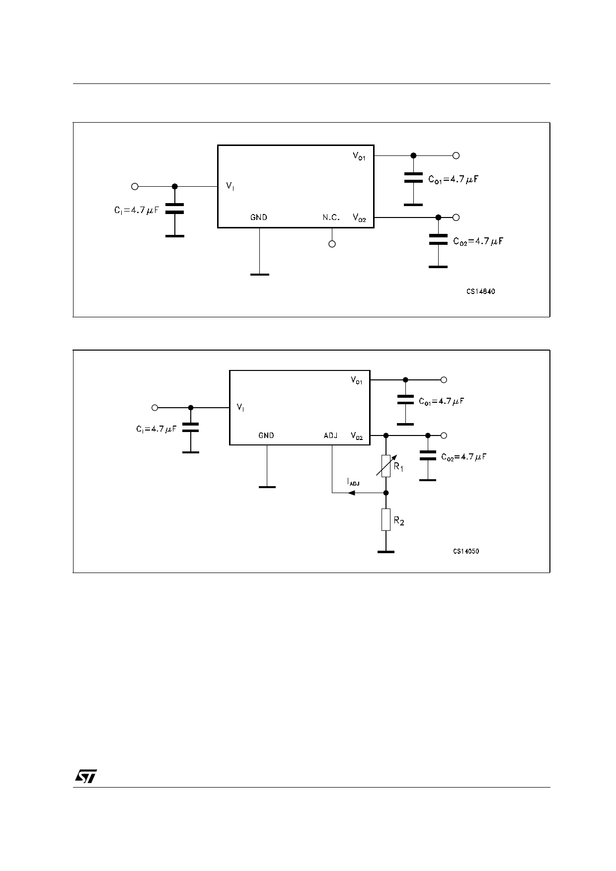
APPLICATION CIRCUIT OF FIXED/FIXED VERSION
ST2L05
APPLICATION CIRCUIT OF FIXED/ADJ VERSION
NOTE: The regulator is designed to be stable with either tantalum or ceramic capacitors on the input and outputs. The expected values of
the input and output X7R ceramic capacitors are from 4.7µF to 22µF with 4.7µF typical. The input capacitor must be connected within 0.5
inches of the VI terminal. The output capacitors must also be connected within 0.5 inches of output pins VO1 and VO2. There is no upper limit
to the size of the input capacitor (for more details see the Application Hints section).
NOTE: In the Fixed/ADJ version, the adjustable output voltage VO2 is designed to support output voltages from 1.25V to VI - VDROP. The
adjustable output voltage VO2 is set by a resistor divider connected between VO2 (pin4) and Ground (pin3) with its centre tap connected to
VO2 ADJ (pin2). The voltage divider resistors are: R1 connected to VO2 and VO2 ADJ and R2 connected to VO2 ADJ and GND. VO2 is deter-
mined by VREF, R1, R2, and IADJ as follows (for more details see the Application Hints section):
VO2 = VREF (1+R1/R2) + IADJR1
5/24
5 Page 
ST2L05
ELECTRICAL CHARACTERISTICS OF FIXED OUTPUT 3.3V (IO = 10mA to 1A, TJ = 0 to 125°C,
VI = 4.5V to 7V, CI = 4.7µF, CO1 = CO2 = 4.7µF, otherwise specified)
Symbol
Parameter
Test Conditions
Min. Typ. Max. Unit
VO Output Voltage 3.3V
IO = 5mA to 1A, VI = 4.75 to 5.25V
T = 25°C
VO Output Voltage 3.3V
IO = 5mA to 1A, VI = 4.75 to 5.25V
∆VO Line Regulation
VI = 4.75 to 5.25V, IO = 5mA to 1A
∆VO Load Regulation
VI = 4.75V, IO = 10mA to 1A
VD Dropout Voltage ∆VO = -1% IO = 1A
IS Current Limit
VI = 5.5V
IOMIN Min Output Current for
regulation
eN RMS Output Noise (1)(4) T = 25°C
SVR
Supply Voltage
Rejection (2)(4)
VI = 5V
∆VO/∆IO
Transient Response
Change of VO with step
load change(3)(4)
VI = 5V, IO = 1mA to 1A, tr ≥ 1µs
VI = 5V, IO = 1A to 1mA, tf ≥ 1µs
∆VO1/∆VI Transient Response
Change of VOUT1 with
application of VI (3)(4)
0 to 5V step input, IO= 1mA to 1A,
tr ≥ 1µs
∆VO/∆IO Transient Response Short
Circuit Removal
Response (3)(4)
VI = 5V, IO = short to IO = 10mA
TR Thermal Regulation (4)
IO = 1A, tPULSE = 30ms
S Temperature Stability (4)
S Long Term Stability (4)
(1000Hrs)
TJ = 125°C
3.234 3.3 3.366 V
3.2 3.3 3.4
15
12
1.3
1
0
0.003
60
V
mV
mV
V
A
mA
%
dB
10(5)
10(5)
10(5)
%
%
20(5)
%
0.1 %/W
0.5 %
0.3 %
NOTE 1: Bandwidth of 10 Hz to 10KHz.
NOTE 2: 120Hz input ripple.
NOTE 3: CI = 20µF, C1 and CO2 = 10µF. CI, CO1 and CO2 are all X7R ceramic capacitors.
NOTE 4: Guaranteed by design, not tested in production.
NOTE 5: % undershoot or overshoot of VO.
11/24
11 Page | ||
| Páginas | Total 24 Páginas | |
| PDF Descargar | [ Datasheet ST2L05.PDF ] | |
Hoja de datos destacado
| Número de pieza | Descripción | Fabricantes |
| ST2L01 | DUAL VOLTAGE REGULATOR | STMicroelectronics |
| ST2L05 | VERY LOW QUIESCENT CURRENT DUAL VOLTAGE REGULATOR | STMicroelectronics |
| Número de pieza | Descripción | Fabricantes |
| SLA6805M | High Voltage 3 phase Motor Driver IC. |
Sanken |
| SDC1742 | 12- and 14-Bit Hybrid Synchro / Resolver-to-Digital Converters. |
Analog Devices |
|
DataSheet.es es una pagina web que funciona como un repositorio de manuales o hoja de datos de muchos de los productos más populares, |
| DataSheet.es | 2020 | Privacy Policy | Contacto | Buscar |
