|
|
|
PDF MC33580 Data sheet ( Hoja de datos )
| Número de pieza | MC33580 | |
| Descripción | Quad High Side Switch | |
| Fabricantes | Motorola Semiconductor | |
| Logotipo | ||
Hay una vista previa y un enlace de descarga de MC33580 (archivo pdf) en la parte inferior de esta página. Total 30 Páginas | ||
|
No Preview Available !
Freescale Semiconductor
Advance Information
Document Number: MC33580
Rev. 6.0, 4/2007
Quad High-Side Switch
(Quad 15 mΩ)
33580
The 33580 is one in a family of devices designed for low-voltage
automotive and industrial lighting and motor control applications. Its
four low RDS(ON) MOSFETs (four 15 mΩ) can control the high sides of
four separate resistive or inductive loads.
Programming, control, and diagnostics are accomplished using a
16-bit SPI interface. Additionally, each output has its own parallel input
for pulse-width modulation (PWM) control if desired. The 33580 allows
the user to program via the SPI the fault current trip levels and duration
of acceptable lamp inrush or motor stall intervals. Such
programmability allows tight control of fault currents and can protect
wiring harnesses and circuit boards as well as loads.
The 33580 is packaged in a power-enhanced 12x 12 nonleaded
Power QFN package with exposed tabs.
HIGH-SIDE SWITCH
Features
www.DataSheet4U.com
• Quad 15 mΩ High-Side Switches (at 25°C)
• Operating Voltage Range of 6.0 V to 27 V with Standby Current
< 5.0 µA
• SPI Control of Overcurrent Limit, Overcurrent Fault Blanking
PNA SUFFIX (Pb-FREE)
98ART10510D
24-PIN PQFN (12 x 12)
Time, Output OFF Open Load Detection, Output ON/OFF
Control, Watchdog Timeout, Slew Rates, and Fault Status
Reporting
ORDERING INFORMATION
• SPI Status Reporting of Overcurrent, Open and Shorted Loads,
Overtemperature, Undervoltage and Overvoltage Shutdown,
Fail-Safe Pin Status, and Program Status
Device
Temperature
Range (TA)
Package
• Analog Current Feedback with Selectable Ratio
MC33580BAPNA/R2 -40°C to 125°C
24 PQFN
• Analog Board Temperature Feedback
• Enhanced -16 V Reverse Polarity VPWR Protection
• Pb-Free Packaging Designated by Suffix Code PNA
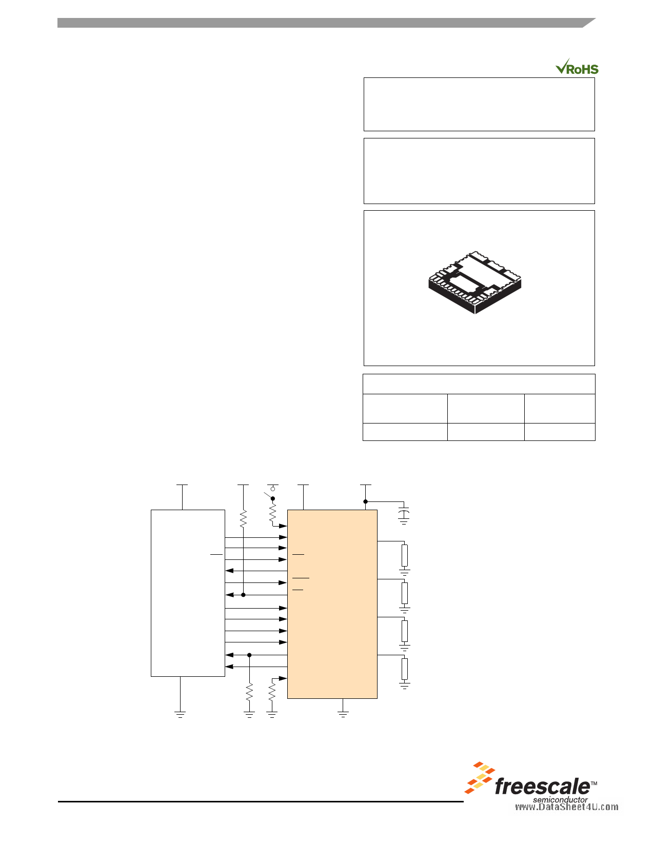
VDD
VDD VPWR VDD
VPWR
SO
SCLK
CS
SI
MCU
I/O
I/O
I/O
I/O
I/O
I/O
A/D
GND A/D
33580
VDD
WAKE
SI
SCLK
CS
SO
RST
FS
IN0
IN1
IN2
IN3
CSNS
TEMP
FSI
VPWR
HS0
HS1
HS2
HS3
GND
GND
LOAD 0
LOAD 1
LOAD 2
LOAD 3
Figure 1. 33580 Simplified Application Diagram
* This document contains certain information on a new product.
Specifications and information herein are subject to change without notice.
© Freescale Semiconductor, Inc., 2007. All rights reserved.
1 page 
ELECTRICAL CHARACTERISTICS
MAXIMUM RATINGS
ELECTRICAL CHARACTERISTICS
MAXIMUM RATINGS
Table 2. Maximum Ratings
All voltages are with respect to ground unless otherwise noted. Exceeding these ratings may cause a malfunction or
permanent damage to the device.
Ratings
Symbol
Value
Unit
ELECTRICAL RATINGS
Operating Voltage Range
Steady-State
VPWR(SS)
-16 to 41
V
VDD Supply Voltage
Input/Output Voltage (1)
SO Output Voltage (1)
WAKE Input Clamp Current
CSNS Input Clamp Current
HS [0:3] Voltage
Positive
Negative
Output Current (2)
Output Clamp Energy (3)
www.DataSheet4U.com ESD Voltage (4)
Human Body Model (HBM)
Charge Device Model (CDM)
Corner Pins (1, 13, 19, 21)
All Other Pins (2-12, 14-18, 20, 22-24)
VDD
See note (1)
VSO
ICL(WAKE)
ICL(CSNS)
VHS
IHS[0:3]
ECL [0:3]
VESD1
VESD2
-0.3 to 5.5
-0.3 to 7.0
-0.3 to VDD+0.3
2.5
10
41
-16
22.8
0.2
± 2000
± 750
± 500
V
V
V
mA
mA
V
A
J
V
THERMAL RATINGS
Operating Temperature
Ambient
Junction
°C
TA -40 to 125
TJ -40 to 150
Storage Temperature
Thermal Resistance (5)
Junction to Case
Junction to Ambient
TSTG
RθJC
RθJA
-55 to 150
<1.0
30
°C
°C/ W
Peak Pin Reflow Temperature During Solder Mounting (6)
TSOLDER
245
°C
Notes
1. Exceeding voltage limits on IN[0:3], RST, FSI, CSNS, TEMP, SI, SO, SCLK, CS, or FS pins may cause a malfunction or permanent
damage to the device.
2. Continuous high-side output current rating so long as maximum junction temperature is not exceeded. Calculation of maximum output
current using package thermal resistance is required.
3. Active clamp energy using single-pulse method (L = 2 mH, RL = 0 Ω, VPWR = 14 V, TJ = 150°C initial).
4. ESD testing is performed in accordance with the Human Body Model (HBM) (CZAP = 100 pF, RZAP = 1500 Ω), the Machine Model (MM)
(CZAP = 200 pF, RZAP = 0 Ω), and the Charge Device Model (CDM), Robotic (CZAP = 4.0pF).
5. Device mounted on a 2s2p test board per JEDEC JESD51-2.
6. Pin soldering temperature limit is for 10 seconds maximum duration. Not designed for immersion soldering. Exceeding these limits may
cause malfunction or permanent damage to the device.
Analog Integrated Circuit Device Data
Freescale Semiconductor
33580
5
5 Page 
ELECTRICAL CHARACTERISTICS
DYNAMIC ELECTRICAL CHARACTERISTICS
Table 4. Dynamic Electrical Characteristics (continued)
Characteristics noted under conditions 6.0 V ≤ VPWR ≤ 27 V, 4.5 V ≤ VDD ≤ 5.5 V, -40°C ≤ TA ≤ 125°C, GND = 0 V unless
otherwise noted. Typical values noted reflect the approximate parameter means at TA = 25°C under nominal conditions unless
otherwise noted.
Characteristic
Symbol
Min Typ Max Unit
POWER OUTPUT TIMING (HS0, HS1, HS2, HS3) (continued)
Output Turn-ON Delay Time in Slow Slew Rate (21)
DICR = 0
Output Turn-ON Delay Time in Fast Slew Rate (21)
DICR = 1
Output Turn-OFF Delay Time in Slow Slew Rate Mode (22)
DICR = 0
Output Turn-OFF Delay Time in Fast Slew Rate Mode (22)
DICR = 1
t DLY_SLOW(ON)
2.0 10 130
t DLY_FAST(ON)
1.0 3.0 60
t DLY_SLOW(OFF)
20
100 400
t DLY_FAST(OFF)
5.0 20 100
µs
µs
µs
µs
Overcurrent Low Detection Blanking Time
OCLT[1:0] : 00
OCLT[1:0] : 01 (23)
OCLT[1:0] : 10
OCLT[1:0] : 11
t OCL0
t OCL1
t OCL2
t OCL3
108
–
55
0.08
155
–
75
0.15
202
–
95
0.3
ms
Overcurrent High Detection Blanking Time
CS to CSNS Valid Time (24)
Watchdog Timeout (25)
www.DataSheet4U.com
WD[1:0] : 00
WD[1:0] : 01
WD[1:0] : 10
WD[1:0] : 11
tOCH
t CNSVAL
t WDTO0
t WDTO1
t WDTO2
t WDTO3
1.0
–
446
223
1800
900
5
–
558
279
2250
1125
20
10
725
363
2925
1463
µs
µs
ms
Notes
21. Turn-ON delay time measured from rising edge of any signal (IN[0:3], SCLK, CS) that would turn the output ON to VHS[0:3] = 0.5 V with
RL = 5.0 Ω resistive load.
22. Turn-OFF delay time measured from falling edge of any signal (IN[0:3], SCLK, CS) that would turn the output OFF to VHS[0:3] = VPWR-
0.5 V with RL = 5.0 Ω resistive load.
23. This logical bit is not defined. Do not use.
24. Time necessary for the CSNS to be with ±5% of the targeted value.
25. Watchdog timeout delay measured from the rising edge of WAKE or RST from a sleep state condition, to output turn-ON with the output
driven OFF and FSI floating. The values shown are for WDR setting of [00]. The accuracy of tWDTO is consistent for all configured
watchdog time-outs.
Analog Integrated Circuit Device Data
Freescale Semiconductor
33580
11
11 Page | ||
| Páginas | Total 30 Páginas | |
| PDF Descargar | [ Datasheet MC33580.PDF ] | |
Hoja de datos destacado
| Número de pieza | Descripción | Fabricantes |
| MC3358 | DUAL DIFFERENTIAL INPUT OPERATIONAL AMPLIFIERS | Motorola Semiconductors |
| MC33580 | Quad High Side Switch | Motorola Semiconductor |
| Número de pieza | Descripción | Fabricantes |
| SLA6805M | High Voltage 3 phase Motor Driver IC. |
Sanken |
| SDC1742 | 12- and 14-Bit Hybrid Synchro / Resolver-to-Digital Converters. |
Analog Devices |
|
DataSheet.es es una pagina web que funciona como un repositorio de manuales o hoja de datos de muchos de los productos más populares, |
| DataSheet.es | 2020 | Privacy Policy | Contacto | Buscar |