|
|
|
PDF AD9271 Data sheet ( Hoja de datos )
| Número de pieza | AD9271 | |
| Descripción | Octal LAN/VGA/AAF/ADC and Crosspoint Switch | |
| Fabricantes | Analog Devices | |
| Logotipo | ||
Hay una vista previa y un enlace de descarga de AD9271 (archivo pdf) en la parte inferior de esta página. Total 30 Páginas | ||
|
No Preview Available !
FEATURES
8 channels of LNA, VGA, AAF, and ADC
Low noise preamplifier (LNA)
Input-referred noise = 1.1 nV/√Hz @ 5 MHz typical,
gain = 18 dB
SPI-programmable gain = 14 dB/15.6 dB/18 dB
Single-ended input; VIN maximum = 400 mV p-p/
333 mV p-p/250 mV p-p
Dual-mode active input impedance matching
Bandwidth (BW) > 70 MHz
Full-scale (FS) output = 2 V p-p differential
Variable gain amplifier (VGA)
Gain range = −6 dB to +24 dB
Linear-in-dB gain control
Antialiasing filter (AAF)
3rd-order Butterworth cutoff
Programmable from 8 MHz to 18 MHz
Analog-to-digital converter (ADC)
12 bits at 10 MSPS to 50 MSPS
SNR = 70 dB
SFDR = 80 dB
Serial LVDS (ANSI-644, IEEE 1596.3 reduced range link)
Data and frame clock outputs
Includes crosspoint switch to support
continuous wave (CW) Doppler
Low power, 150 mW per channel at 12 bits/40 MSPS (TGC)
90 mW per channel in CW Doppler
Single 1.8 V supply (3.3 V supply for CW Doppler output bias)
Flexible power-down modes
Overload recovery in <10 ns
Fast recovery from low power standby mode, <2 μs
100-lead TQFP
APPLICATIONS
Medical imaging/ultrasound
Automotive radar
GENERAL DESCRIPTION
The AD9271 is designed for low cost, low power, small size,
and ease of use. It contains eight channels of a variable gain amp-
lifier (VGA) with low noise preamplifier (LNA); an antialiasing
filter (AAF); and a 12-bit, 10 MSPS to 50 MSPS analog-to-digital
converter (ADC).
Each channel features a variable gain range of 30 dB, a fully
differential signal path, an active input preamplifier termination, a
maximum gain of up to 40 dB, and an ADC with a conversion
rate of up to 50 MSPS. The channel is optimized for dynamic
performance and low power in applications where a small
package size is critical.
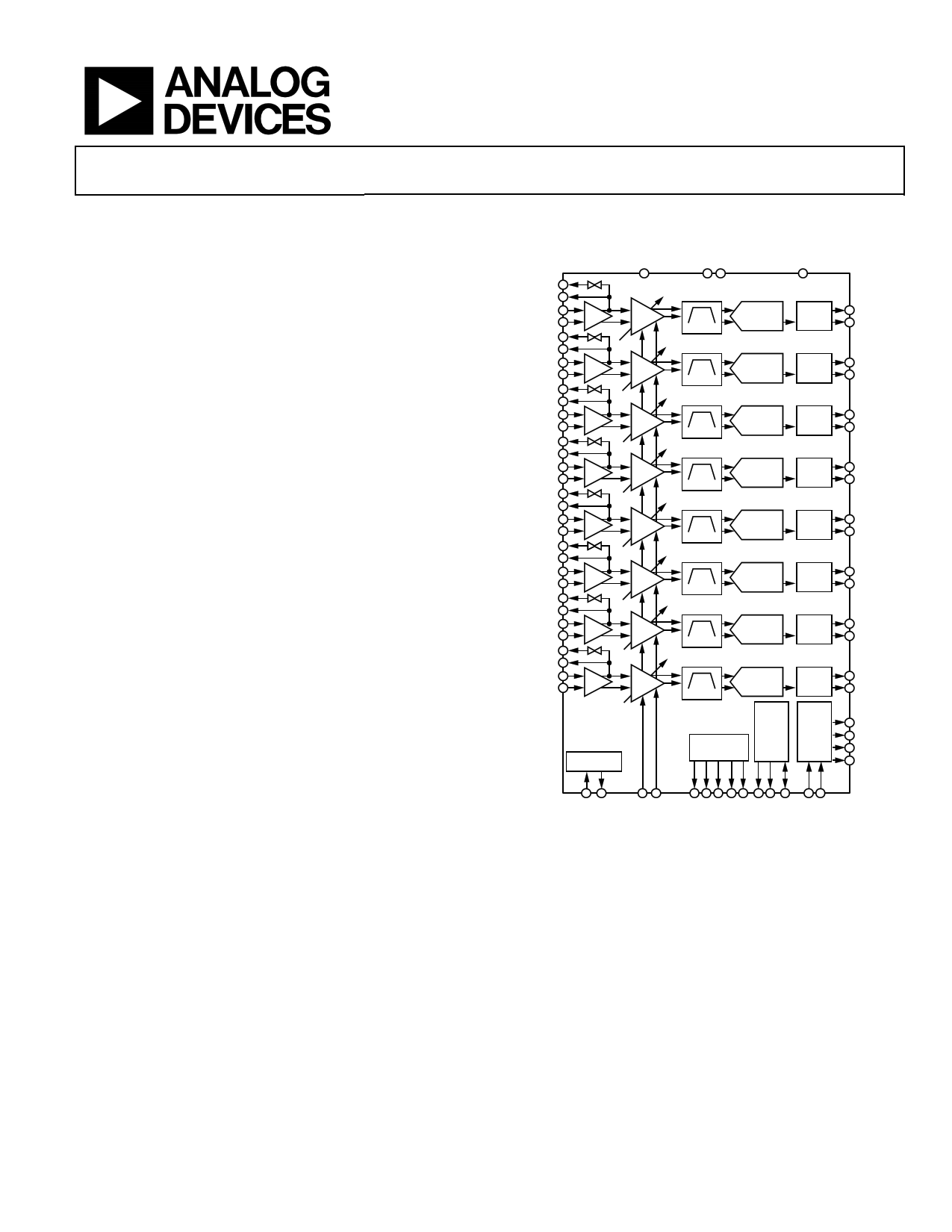
Octal LNA/VGA/AAF/ADC
and Crosspoint Switch
AD9271
FUNCTIONAL BLOCK DIAGRAM
LOSW-A
LO-A
LI-A
LNA VGA
LG-A
LOSW-B
LO-B
LI-B
LG-B LNA VGA
LOSW-C
LO-C
LI-C
LG-C LNA VGA
LOSW-D
LO-D
LI-D LNA VGA
LG-D
LOSW-E
LO-E
LI-E
LG-E LNA VGA
LOSW-F
LO-F
LI-F
LG-F LNA VGA
LOSW-G
LO-G
LI-G
LNA VGA
LG-G
LOSW-H
LO-H
LI-H
LG-H LNA VGA
SWITCH
ARRAY
AD9271
AAF
12-BIT
ADC
SERIAL
LVDS
DOUTA+
DOUTA–
AAF
12-BIT
ADC
SERIAL
LVDS
DOUTB+
DOUTB–
AAF
12-BIT
ADC
SERIAL
LVDS
DOUTC+
DOUTC–
AAF
12-BIT
ADC
SERIAL
LVDS
DOUTD+
DOUTD–
AAF
12-BIT
ADC
SERIAL
LVDS
DOUTE+
DOUTE–
AAF
12-BIT
ADC
SERIAL
LVDS
DOUTF+
DOUTF–
AAF
12-BIT
ADC
SERIAL
LVDS
DOUTG+
DOUTG–
AAF
12-BIT
ADC
REFERENCE
SERIAL
LVDS
DOUTH+
DOUTH–
FCO+
FCO–
DCO+
DCO–
Figure 1.
The LNA has a single-ended-to-differential gain that is selectable
through the SPI. The LNA input noise is typically 1.2 nV/√Hz,
and the combined input-referred noise of the entire channel
is 1.4 nV/√Hz at maximum gain. Assuming a 15 MHz noise
bandwidth (NBW) and a 15.6 dB LNA gain, the input SNR is
roughly 86 dB. In CW Doppler mode, the LNA output drives a
transconductance amp that is switched through an 8 × 6
differential crosspoint switch. The switch is programmable
through the SPI.
Rev. B
Information furnished by Analog Devices is believed to be accurate and reliable. However, no
responsibility is assumed by Analog Devices for its use, nor for any infringements of patents or other
rights of third parties that may result from its use. Specifications subject to change without notice. No
license is granted by implication or otherwise under any patent or patent rights of Analog Devices.
Trademarksandregisteredtrademarksarethepropertyoftheirrespectiveowners.
One Technology Way, P.O. Box 9106, Norwood, MA 02062-9106, U.S.A.
Tel: 781.329.4700
www.analog.com
Fax: 781.461.3113 ©2007–2009 Analog Devices, Inc. All rights reserved.
1 page 
AD9271
SPECIFICATIONS
AC SPECIFICATIONS
AVDD = 1.8 V, DRVDD = 1.8 V, CWVDD = 3.3 V, 1.0 V internal ADC reference, fIN = 5 MHz, RS = 50 Ω, LNA gain = 15.6 dB (6), AAF
LPF cutoff = 1/3 × fS, HPF cutoff = 700 kHz, full temperature, unless otherwise noted.
Table 1.
Parameter 1
Conditions
AD9271-25
Min Typ
Max
LNA CHARACTERISTICS
Gain = 5/6/8
Single-ended input
to differential output
14/15.6/18
Single-ended input
to single-ended
output
8/9.6/12
Input Voltage Range,
Gain = 5/6/8
LNA output limited
to 2 V p-p differential
output
400/333/250
Input Common
Mode
1.4
Input Resistance
RFB = 200 Ω
50
RFB = 400 Ω
100
RFB = ∞
15
Input Capacitance
LI-x
15
−3 dB Bandwidth
40
Input Noise Current,
Gain = 5/6/8
1.1
Input Noise Voltage, RS = 0 Ω, RFB = ∞
Gain = 5/6/8
1.4/1.4/1.3
1 dB Input
Compression
Point, Gain = 5/6/8
VGAIN = 0 V
770/650/495
Noise Figure
Active Termination RS = 50 Ω, RFB = 200 Ω
Match
6.7
Unterminated
RFB = ∞
4.9
FULL-CHANNEL (TGC)
CHARACTERISTICS
AAF High-Pass Cutoff −3 dB
DC/350/700
AAF Low-Pass Cutoff −3 dB, programmable
1/3 × fSAMPLE
(8 to 18)
Bandwidth Tolerance
±15
Group Delay Variation f = 1 to 18 MHz,
gain = 0 V to 1 V
±2
Input-Referred Noise LNA gain = 5/6/8,
Voltage
RFB = ∞
1.7/1.6/1.5
Correlated Noise Ratio No signal, correlated/
uncorrelated
−30
Output Offset
AAF high pass =
700 kHz
−50
+50
Signal-to-Noise Ratio
(SNR)
fIN = 5 MHz
at −7 dBFS
VGAIN = 0 V
65.8
fIN = 5 MHz
at −1 dBFS
VGAIN = 1 V
62
AD9271-40
Min Typ
Max
14/15.6/18
8/9.6/12
400/333/250
1.4
50
100
15
15
60
1.1
1.3/1.2/1.1
770/650/495
6.7
4.4
DC/350/700
1/3 × fSAMPLE
(8 to 18)
±15
±2
1.6/1.4/1.3
−30
−35 +35
64.4
59.7
AD9271-50
Min Typ
Max
14/15.6/18
8/9.6/12
400/333/250
1.4
50
100
15
15
70
1.1
1.3/1.2/1.1
770/650/495
6.7
4.2
DC/350/700
1/3 × fSAMPLE
(8 to 18)
±15
±2
1.6/1.4/1.2
−30
−35 +35
63.7
59
Unit
dB
dB
mV p-p
SE2
V
Ω
Ω
kΩ
pF
MHz
pA/√Hz
nV/√Hz
mV p-p
dB
dB
kHz
MHz
%
ns
nV/√Hz
dB
LSB
dBFS
dBFS
Rev. B | Page 4 of 60
5 Page 
AD9271
ABSOLUTE MAXIMUM RATINGS
Table 4.
Parameter
ELECTRICAL
AVDD
DRVDD
CWVDD
GND
AVDD
Digital Outputs
(DOUTx+, DOUTx−,
DCO+, DCO−,
FCO+, FCO−)
CLK+, CLK−
LI-x
LO-x
LOSW-x
CWDx−, CWDx+
SDIO, GAIN+, GAIN−
PDWN, STBY, SCLK, CSB
REFT, REFB, RBIAS
VREF, SENSE
ENVIRONMENTAL
Operating Temperature
Range (Ambient)
Storage Temperature
Range (Ambient)
Maximum Junction
Temperature
Lead Temperature
(Soldering, 10 sec)
With
Respect To Rating
GND
GND
GND
GND
DRVDD
GND
−0.3 V to +2.0 V
−0.3 V to +2.0 V
−0.3 V to +3.9 V
−0.3 V to +0.3 V
−2.0 V to +2.0 V
−0.3 V to +2.0 V
GND
LG-x
LG-x
LG-x
GND
GND
GND
GND
GND
−0.3 V to +3.9 V
−0.3 V to +2.0 V
−0.3 V to +2.0 V
−0.3 V to +2.0 V
−0.3 V to +3.9 V
−0.3 V to +2.0 V
−0.3 V to +3.9 V
−0.3 V to +2.0 V
−0.3 V to +2.0 V
−40°C to +85°C
−65°C to +150°C
150°C
300°C
Stresses above those listed under Absolute Maximum Ratings
may cause permanent damage to the device. This is a stress
rating only; functional operation of the device at these or any
other conditions above those indicated in the operational
section of this specification is not implied. Exposure to absolute
maximum rating conditions for extended periods may affect
device reliability.
THERMAL IMPEDANCE
Table 5.
Air Flow Velocity (m/s)
0.0
1.0
2.5
θJA1 θJB θJC Unit
20.3 °C/W
14.4 7.6 4.7 °C/W
12.9 °C/W
1 θJA for a 4-layer PCB with solid ground plane (simulated). Exposed pad
soldered to PCB.
ESD CAUTION
Rev. B | Page 10 of 60
11 Page | ||
| Páginas | Total 30 Páginas | |
| PDF Descargar | [ Datasheet AD9271.PDF ] | |
Hoja de datos destacado
| Número de pieza | Descripción | Fabricantes |
| AD9271 | Octal LAN/VGA/AAF/ADC and Crosspoint Switch | Analog Devices |
| AD9272 | Octal LNA/VGA/AAF/ADC and Crosspoint Switch | Analog Devices |
| AD9273 | Octal LNA/VGA/AAF/ADC and Crosspoint Switch | Analog Devices |
| AD9276 | Octal LNA/VGA/AAF/12-Bit ADC and CW I/Q Demodulator | Analog Devices |
| Número de pieza | Descripción | Fabricantes |
| SLA6805M | High Voltage 3 phase Motor Driver IC. |
Sanken |
| SDC1742 | 12- and 14-Bit Hybrid Synchro / Resolver-to-Digital Converters. |
Analog Devices |
|
DataSheet.es es una pagina web que funciona como un repositorio de manuales o hoja de datos de muchos de los productos más populares, |
| DataSheet.es | 2020 | Privacy Policy | Contacto | Buscar |