|
|
|
PDF AD9949 Data sheet ( Hoja de datos )
| Número de pieza | AD9949 | |
| Descripción | 12-Bit CCD Signal Processor | |
| Fabricantes | Analog Devices | |
| Logotipo | ||
Hay una vista previa y un enlace de descarga de AD9949 (archivo pdf) en la parte inferior de esta página. Total 30 Páginas | ||
|
No Preview Available !
FEATURES
New AD9949A supports CCD line length > 4096 pixels
Correlated double sampler (CDS)
0 dB to 18 dB pixel gain amplifier (PxGA®)
6 dB to 42 dB 10-bit variable gain amplifier (VGA)
12-bit, 36 MSPS analog-to-digital converter (ADC)
Black level clamp with variable level control
Complete on-chip timing driver
Precision Timing™ core with < 600 ps resolution
On-chip 3 V horizontal and RG drivers
40-lead LFCSP package
APPLICATIONS
Digital still cameras
High speed digital imaging applications
12-Bit CCD Signal Processor with
Precision Timing Core
AD9949
GENERAL DESCRIPTION
The AD9949 is a highly integrated CCD signal processor for
digital still camera applications. Specified at pixel rates of up to
36 MHz, the AD9949 consists of a complete analog front end
with A/D conversion, combined with a programmable timing
driver. The Precision Timing core allows adjustment of high
speed clocks with < 600 ps resolution.
The analog front end includes black level clamping, CDS,
PxGA, VGA, and a 36 MSPS, 12-bit ADC. The timing driver
provides the high speed CCD clock drivers for RG and H1 to
H4. Operation is programmed using a 3-wire serial interface.
Packaged in a space-saving, 40-lead LFCSP package, the
AD9949 is specified over an operating temperature range of
−20°C to +85°C.
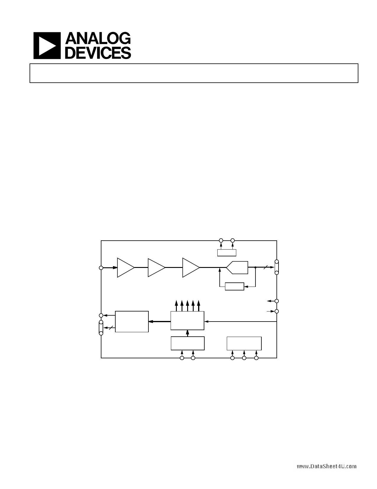
FUNCTIONAL BLOCK DIAGRAM
REFT REFB
CCDIN
CDS
0dB TO 18dB
PxGA
6dB TO 42dB
VGA
VREF
12-BIT
ADC
12
DOUT
RG
H1 TO H4
HORIZONTAL
4 DRIVERS
AD9949
INTERNAL
CLOCKS
PRECISION
TIMING
CORE
SYNC
GENERATOR
HD VD
Figure 1.
CLAMP
HBLK
CLP/PBLK
CLI
INTERNAL
REGISTERS
SL SCK SDATA
Rev. B
Information furnished by Analog Devices is believed to be accurate and reliable.
However, no responsibility is assumed by Analog Devices for its use, nor for any
infringements of patents or other rights of third parties that may result from its use.
Specifications subject to change without notice. No license is granted by implication
or otherwise under any patent or patent rights of Analog Devices. Trademarks and
registered trademarks are the property of their respective owners.
One Technology Way, P.O. Box 9106, Norwood, MA 02062-9106, U.S.A.
Tel: 781.329.4700
www.analog.com
Fax: 781.326.8703 © 2004 Analog Devices, Inc. All rights reserved.
1 page 
AD9949
TIMING SPECIFICATIONS
CL = 20 pF, fCLI = 36 MHz, unless otherwise noted.
Table 4.
Parameter
MASTER CLOCK (CLI) (See Figure 16)
CLI Clock Period
CLI High/Low Pulse Width
Delay from CLI to Internal Pixel Period Position
CLPOB PULSE WIDTH (PROGRAMMABLE)1
SAMPLE CLOCKS (See Figure 18)
SHP Rising Edge to SHD Rising Edge
DATA OUTPUTS (See Figure 19 and Figure 20)
Output Delay From Programmed Edge
Pipeline Delay
SERIAL INTERFACE (SERIAL TIMING SHOWN IN Figure 14 and Figure 15)
Maximum SCK Frequency
SL to SCK Setup Time
SCK to SL Hold Time
SDATA Valid to SCK Rising Edge Setup
SCK Falling Edge to SDATA Valid Hold
SCK Falling Edge to SDATA Valid Read
Symbol
tCLI
tADC
tCLIDLY
tCOB
tS1
tOD
fSCLK
tLS
tLH
tDS
tDH
tDV
Min Typ Max Unit
27.8
11.2 13.9 16.6
6
2 20
ns
ns
ns
Pixels
12.5 13.9
ns
6 ns
11 Cycles
10 MHz
10 ns
10 ns
10 ns
10 ns
10 ns
1 Minimum CLPOB pulse width is for functional operation only. Wider typical pulses are recommended to achieve low noise clamp reference.
Rev. B | Page 5 of 36
5 Page 
SYSTEM OVERVIEW
CCD
V-DRIVER
V1 TO Vx, VSG1 TO VSGx, SUBCK
H1 TO H4, RG
DOUT
CCDIN
AD9949
INTEGRATED
AFE + TD
HD, VD
DIGITAL IMAGE
PROCESSING
ASIC
SERIAL
INTERFACE
CLI
Figure 11. Typical Application
Figure 11 shows the typical system application diagram for the
AD9949. The CCD output is processed by the AD9949’s AFE
circuitry, which consists of a CDS, a PxGA, a VGA, a black level
clamp, and an ADC. The digitized pixel information is sent to
the digital image processor chip where all postprocessing and
compression occurs. To operate the CCD, CCD timing
parameters are programmed into the AD9949 from the image
processor through the 3-wire serial interface. From the system
master clock, CLI, provided by the image processor, the
AD9949 generates the high speed CCD clocks and all internal
AFE clocks. All AD9949 clocks are synchronized with VD and
HD. The AD9949’s horizontal pulses (CLPOB, PBLK, and
HBLK) are programmed and generated internally.
The H-drivers for H1 to H4 and RG are included in the
AD9949, allowing these clocks to be directly connected to the
CCD. The H-drive voltage of 3 V is supported in the AD9949.
Figure 12 shows the horizontal and vertical counter dimensions
for the AD9949. All internal horizontal clocking is programmed
using these dimensions to specify line and pixel locations.
AD9949
H-COUNTER BEHAVIOR
When the maximum horizontal count of 4096 pixels is
exceeded, the H-counter in the AD9949 rolls over to zero and
continues counting. It is, therefore, recommended that the
maximum counter value not be exceeded.
However, the newer AD9949A version behaves differently. In
the AD9949A, the internal H-counter holds at its maximum
count of 4095 instead of rolling over. This feature allows the
AD9949A to be used in applications containing a line length
greater than 4096 pixels. Although no programmable values for
the horizontal blanking or clamping are available beyond pixel
4095, the H, RG, and AFE clocking continues to operate,
sampling the remaining pixels on the line.
MAXIMUM FIELD DIMENSIONS
12-BIT HORIZONTAL = 4096 PIXELS MAX
12-BIT VERTICAL = 4096 LINES MAX
Figure 12. Vertical and Horizontal Counters
MAX VD LENGTH IS 4095 LINES
VD
MAX HD LENGTH IS 4095 PIXELS
HD
CLI
Figure 13. Maximum VD/HD Dimensions
Rev. B | Page 11 of 36
11 Page | ||
| Páginas | Total 30 Páginas | |
| PDF Descargar | [ Datasheet AD9949.PDF ] | |
Hoja de datos destacado
| Número de pieza | Descripción | Fabricantes |
| AD9940 | Correlated Double Sampler | Analog Devices |
| AD9941 | 56 MSPS Imaging Signal Processor | Analog Devices |
| AD9942 | 14-Bit CCD Signal Processor | Analog Devices |
| AD9943 | CCD Signal Processors | Analog Devices |
| Número de pieza | Descripción | Fabricantes |
| SLA6805M | High Voltage 3 phase Motor Driver IC. |
Sanken |
| SDC1742 | 12- and 14-Bit Hybrid Synchro / Resolver-to-Digital Converters. |
Analog Devices |
|
DataSheet.es es una pagina web que funciona como un repositorio de manuales o hoja de datos de muchos de los productos más populares, |
| DataSheet.es | 2020 | Privacy Policy | Contacto | Buscar |