|
|
PDF L6701 Data sheet ( Hoja de datos )
| Número de pieza | L6701 | |
| Descripción | 3 Phase Controller | |
| Fabricantes | STMicroelectronics | |
| Logotipo |  |
|
Hay una vista previa y un enlace de descarga de L6701 (archivo pdf) en la parte inferior de esta página. Total 30 Páginas | ||
|
No Preview Available !
L6701
3 Phase Controller for VR10, VR9 and K8 CPUs
Features
■ MULTI-DAC: VR9, VR10 AND K8 DAC
SELECTABLE THROUGH SINGLE PIN
■ 0.7% OUTPUT VOLTAGE ACCURACY
■ ADJUSTABLE REFERENCE OFFSET
■ HIGH CURRENT INTEGRATED DRIVERS
■ DYNAMIC VID MANAGEMENT
■ ACCURATE FULLY-DIFFERENTIAL LOAD-
LINE CURRENT-SENSE ACROSS MAIN
INDUCTORS MAKES BOM INDEPENDENT
ON THE LAYOUT
■ PRECISE CURRENT-SHARING AND OCP
ACROSS LS MOSFETS
■ CONSTANT OVER-CURRENT PROTECTION
■ FEEDBACK DISCONNECTION
PROTECTION
■ PRELIMINARY OV PROTECTION
■ OSCILLATOR INTERNALLY FIXED AT
100kHz (300kHz RIPPLE) EXT ADJUSTABLE
■ SS_END / PGOOD SIGNAL
■ INTEGRATED REMOTE-SENSE BUFFER
■ PWSSO36 PACKAGE WITH EXPOSED PAD
Applications
■ HIGH CURRENT VRM / VRD FOR DESKTOP
/ SERVER/ WORKSTATION CPUs
■ HIGH DENSITY DC / DC CONVERTERS
PowerSSO-36
Description
L6701 is an extremely simple, low-cost solution to
implement a three phase step-down controller
with integrated high-current drivers in a compact
PowerSSO-36 package with exposed pad.
The device embeds three selectable DACs: with a
single pin it is possible to program the device to
work in compatibility with VR9, VR10 or K8
applications managing D-VID with ±0.7% output
voltage accuracy over line and temperature
variations. Additional programmable offset can be
added to the reference voltage with a single
external resistor.
Fast protection against load over current let the
system works in Constant Current mode until
UVP. Preliminary OVP allows full load protection
in case of startup with failed HS. Furthermore,
feedback disconnection prevents from damaging
the load in case of misconnections in the system
board.
Combined use of DCR and RDS(on) current
sensing assures precision in voltage positioning
and safe current sharing and OCP per each
phase.
Order codes
Part number
L6701
L6701TR
December 2005
Package
PowerSSO-36
PowerSSO-36
Packing
Tube
Tape & Reel
Rev 1
1/44
www.st.com
44
1 page 
L6701
2 Pins description and connection diagrams
2 Pins description and connection diagrams
Figure 1. Pins connection (Top view)
SGND
VCC
LGATE1
PGND
LGATE2
LGATE3
BOOT1
UGATE1
PHASE1
BOOT2
UGATE2
PHASE2
BOOT3
UGATE3
PHASE3
SSEND / PGOOD
DAC_SEL
OSC / EN / FAULT
1
2
3
4
5
6
7
8
9
10
11
12
13
14
15
16
17
18
36 COMP
35 FB
34 VSEN
33 CS-
32 CS+
31 ISEN1
30 ISEN2
29 ISEN3
28 FBG
27 FBR
26 VID5
25 VID0
24 VID1
23 VID2
22 VID3
21 VID4
20 REF_OUT
19 REF_IN
2.1 Pin description
Table 1. Pins description
Pin n°
Name
Function
1
SGND
All the internal references are referred to this pin. Connect to the PCB Signal
Ground.
Device Power Supply and LS driver supply.
2 VCC
Operative voltage is 12V ±15%. Filter with at least 1µF MLCC vs. ground.
Channel 1 LS Driver Output.
3 LGATE1
A small series resistor helps in reducing device-dissipated power.
4
PGND
LS Drivers return path. Connect to Power ground Plane.
Channel 2 LS Driver Output.
5 LGATE2
A small series resistor helps in reducing device-dissipated power.
Channel 3 LS Driver Output.
6 LGATE3
A small series resistor helps in reducing device-dissipated power.
Channel 1 HS driver supply.
Connect through a capacitor (100nF typ.) to PHASE1 and provide necessary
7 BOOT1 Bootstrap diode.
A small series resistor upstream the boot diode helps in reducing Boot capacitor
overcharge.
Channel 1 HS driver output.
8 UGATE1
A small series resistors helps in reducing device-dissipated power.
Channel 1 HS driver return path.
9 PHASE1 It must be connected to the HS1 MOSFET source and provides return path for
the HS driver of channel 1.
5/44
5 Page 
L6701
5 Typical application circuit and block diagram
5 Typical application circuit and block diagram
5.1 Application circuit
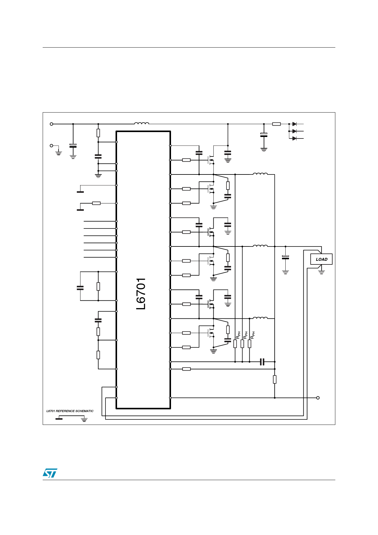
Figure 2. Typical application circuit
VIN LIN
GNDIN
COS
ROS
CF
RF
RFB
L6701 REFERENCE SCHEMATIC
2
VCC
7
BOOT1
4
PGND
1
SGND
17
DAC_SEL
8
UGATE1
9
PHASE1
3
LGATE1
18
OSC/EN/FAULT
31
ISEN1
RISEN
26
VID5
21
VID4
22
VID3
23
VID2
24
VID1
25
VID0
19
REF_IN
10
BOOT2
11
UGATE2
12
PHASE2
5
LGATE2
30
ISEN2
RISEN
20
REF_OUT
36
COMP
13
BOOT3
14
UGATE3
15
PHASE3
35
FB
6
LGATE3
29
ISEN3
RISEN
34
VSEN
32
CS+
33
CS-
27
FBR
28
FBG
16
SSEND / PGOOD
RD
VIN
HS1
LS1
VIN
HS2
LS2
VIN
HS3
LS3
CIN
L1
to BOOT1
to BOOT2
to BOOT3
L2 Vcc_core
COUT
LOAD
L3
CPH
PGOOD
11/44
11 Page | ||
| Páginas | Total 30 Páginas | |
| PDF Descargar | [ Datasheet L6701.PDF ] | |
Hoja de datos destacado
| Número de pieza | Descripción | Fabricantes |
| L6701 | 3 Phase Controller | STMicroelectronics |
| L6706 | Single-phase Switching DC-DC Controllers & Smart Regulators | ST Microelectronics |
| Número de pieza | Descripción | Fabricantes |
| SLA6805M | High Voltage 3 phase Motor Driver IC. |
Sanken |
| SDC1742 | 12- and 14-Bit Hybrid Synchro / Resolver-to-Digital Converters. |
Analog Devices |
|
DataSheet.es es una pagina web que funciona como un repositorio de manuales o hoja de datos de muchos de los productos más populares, |
| DataSheet.es | 2020 | Privacy Policy | Contacto | Buscar |
