|
|
|
PDF ST68C554 Data sheet ( Hoja de datos )
| Número de pieza | ST68C554 | |
| Descripción | (ST68C454 / ST68C554) QUAD UNIVERSAL ASYNCHRONOUS RECEIVER/TRANSMITTER | |
| Fabricantes | Exar Corporation | |
| Logotipo | ||
Hay una vista previa y un enlace de descarga de ST68C554 (archivo pdf) en la parte inferior de esta página. Total 30 Páginas | ||
|
No Preview Available !
ST16C454
ST68C454
QUAD UNIVERSAL ASYNCHRONOUS
RECEIVER/TRANSMITTER (UART)
DESCRIPTION
The ST16C454 is a universal asynchronous receiver
and transmitter (UART) with a dual foot print interface.
The 454 is an enhanced UART with data rates up to
1.5Mbps and software compatible to ST16C450.
Onboard status registers provide the user with error
indications and operational status, modem interface
control. System interrupts may be tailored to meet
user requirements. An internal loop-back capability
allows onboard diagnostics. The ST16C454 offer an
additional 68 mode which allows easy integration with
Motorola, and other popular microprocessors. The
454 combines the package interface modes of the
ST16C454 and ST68C454 series on a single inte-
grated chip.
FEATURES
-DSRA 10
-CTSA 11
-DTRA 12
VCC 13
-RTSA 14
INTA 15
-CSA 16
TXA 17
-IOW 18
TXB 19
-CSB 20
INTB 21
-RTSB 22
GND 23
-DTRB 24
-CTSB 25
-DSRB 26
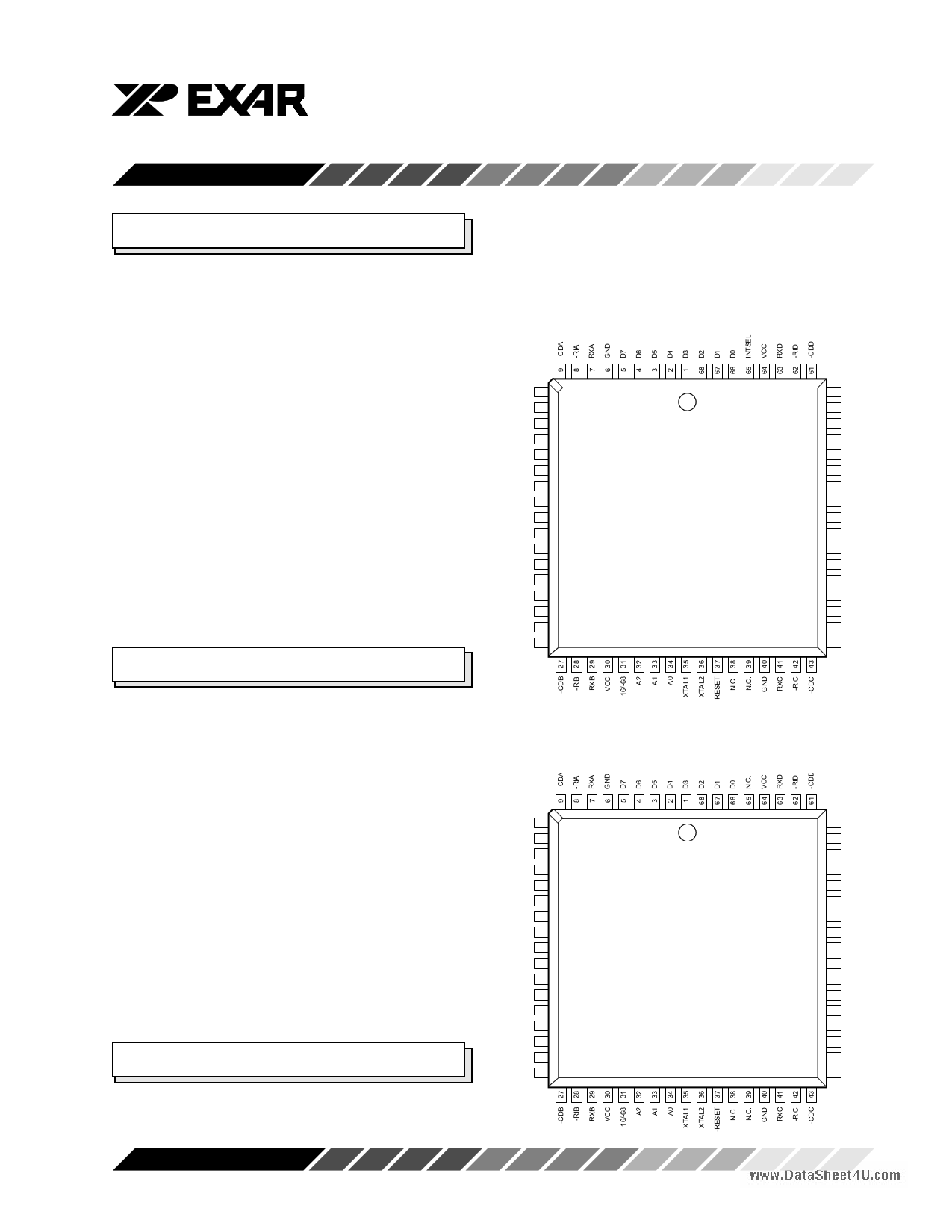
PLCC Package
ST16C454CJ68
16 MODE
60 -DSRD
59 -CTSD
58 -DTRD
57 GND
56 -RTSD
55 INTD
54 -CSD
53 TXD
52 -IOR
51 TXC
50 -CSC
49 INTC
48 -RTSC
47 VCC
46 -DTRC
45 -CTSC
44 -DSRC
• Software compatibility with the Industry Standard
16C450
• 1.5 Mbps transmit/receive operation (24MHz)
• Independent transmit and receive control
• Software selectable Baud Rate Generator
• Modem control signals (-CTS, -RTS, -DSR, -DTR,
-RI, -CD)
• Programmable character lengths (5, 6, 7, 8)
• Even, odd, or no parity bit generation and detection
• Internal loop-back diagnostics
• TTL compatible inputs, outputs
• Low power
ORDERING INFORMATION
-DSRA 10
-CTSA 11
-DTRA 12
VCC 13
-RTSA 14
-IRQ 15
-CS 16
TXA 17
R/-W 18
TXB 19
A3 20
N.C. 21
-RTSB 22
GND 23
-DTRB 24
-CTSB 25
-DSRB 26
ST16C454CJ68
68 MODE
60 -DSRD
59 -CTSD
58 -DTRD
57 GND
56 -RTSD
55 N.C.
54 N.C.
53 TXD
52 N.C.
51 TXC
50 A4
49 N.C.
48 -RTSC
47 VCC
46 -DTRC
45 -CTSC
44 -DSRC
Part number
ST16C454CJ68
ST16C454IJ68
Pins Package
68 PLCC
68 PLCC
Operating temperature
0° C to + 70° C
-40° C to + 85° C
Rev. 3.20
EXAR Corporation, 48720 Kato Road, Fremont, CA 94538 • (510) 668-7000 • FAX (510) 668-7017
1 page 
ST16C454/68C454
SYMBOL DESCRIPTION
Symbol
D0-D2
D3-D7
GND
GND
INT A-B
INT C-D
INTSEL
-IOR
-IOW
Rev. 3.20
Pin
66-68
1-5
6,23
40,57
15,21
49,55
65
52
18
Signal
type
I/O
Pin Description
Data Bus (Bi-directional) - These pins are the eight bit, three state
data bus for transferring information to or from the controlling
CPU. D0 is the least significant bit and the first data bit in a transmit
or receive serial data stream.
Pwr Signal and power ground.
O Interrupt A, B, C, D (active high) - This function is associated with
the 16 mode only. These pins provide individual channel inter-
rupts, INT A-D. INT A-D are enabled when MCR bit-3 is set to a
logic 1, interrupts are enabled in the interrupt enable register (IER),
and when an interrupt condition exists. Interrupt conditions in-
clude: receiver errors, available receiver buffer data, transmit
buffer empty, or when a modem status flag is detected. When the
68 mode is selected, the functions of these pins are reassigned. 68
mode functions are described under the their respective name/pin
headings.
I Interrupt Select. (active high, with internal pull-down) - This
function is associated with the 16 mode only. When the 16 mode
is selected, this pin can be used in conjunction with MCR bit-3 to
enable or disable the three state interrupts, INT A-D or override
MCR bit-3 and force continuous interrupts. Interrupt outputs are
enabled continuously by making this pin a logic 1. Making this pin
a logic 0 allows MCR bit-3 to control the three state interrupt output.
In this mode, MCR bit-3 is set to a logic 1 to enable the three state
outputs. This pin is disabled in the 68 mode.
I Read strobe. (active low Strobe) - This function is associated with
the 16 mode only. A logic 0 transition on this pin will load the
contents of an Internal register defined by address bits A0-A2 onto
the ST16C454 data bus (D0-D7) for access by an external CPU.
This pin is disabled in the 68 mode.
I Write strobe. (active low strobe) - This function is associated with
the 16 mode only. A logic 0 transition on this pin will transfer the
contents of the data bus (D0-D7) from the external CPU to an
internal register that is defined by address bits A0-A2. When the
16 mode is selected, this pin functions as R/-W, see definition
5
5 Page 
ST16C454/68C454
Programmable Baud Rate Generator
The 454 supports high speed modem technologies
that have increased input data rates by employing
data compression schemes. For example a 33.6Kbps
modem that employs data compression may require a
115.2Kbps input data rate. A 128.0Kbps ISDN modem
that supports data compression may need an input
data rate of 460.8Kbps. The 454 can support a stan-
dard data rate of 921.6Kbps.
Single baud rate generator is provided for the trans-
mitter and receiver, allowing independent TX/RX
channel control. The programmable Baud Rate Gen-
erator is capable of accepting an input clock up to 24
MHz, as required for supporting a 1.5Mbps data rate.
The 454 can be configured for internal or external
clock operation. For internal clock oscillator opera-
tion, an industry standard microprocessor crystal (par-
allel resonant/ 22-33 pF load) is connected externally
between the XTAL1 and XTAL2 pins (see figure 8).
Alternatively, an external clock can be connected to
the XTAL1 pin to clock the internal baud rate generator
for standard or custom rates. (see Baud Rate Genera-
tor Programming).
The generator divides the input 16X clock by any
divisor from 1 to 216 -1. The 454 divides the basic
crystal or external clock by 16. Further division of this
16X clock provides two table rates to support low and
high data rate applications using the same system
design. Customized Baud Rates can be achieved by
selecting the proper divisor values for the MSB and
LSB sections of baud rate generator.
Programming the Baud Rate Generator Registers
DLM (MSB) and DLL (LSB) provides a user capability
for selecting the desired final baud rate. The example
in Table 5 below, shows the two selectable baud rate
tables available when using a 1.8432MHz or 7.3728
MHz crystal.
Output
Output
Baud Rate Baud Rate
(1.8432 MHz (7.3728 MHz
Clock)
Clock)
User
16 x Clock
Divisor
(Decimal)
User
16 x Clock
Divisor
(HEX)
DLM
Program
Value
(HEX)
50
300
600
1200
2400
4800
9600
19.2k
38.4k
57.6k
115.2k
200
1200
2400
4800
9600
19.2K
38.4k
76.8k
153.6k
230.4k
460.8k
2304
384
192
96
48
24
12
6
3
2
1
900
180
C0
60
30
18
0C
06
03
02
01
09
01
00
00
00
00
00
00
00
00
00
DLL
Program
Value
(HEX)
00
80
C0
60
30
18
0C
06
03
02
01
Rev. 3.20
11
11 Page | ||
| Páginas | Total 30 Páginas | |
| PDF Descargar | [ Datasheet ST68C554.PDF ] | |
Hoja de datos destacado
| Número de pieza | Descripción | Fabricantes |
| ST68C554 | (ST68C454 / ST68C554) QUAD UNIVERSAL ASYNCHRONOUS RECEIVER/TRANSMITTER | Exar Corporation |
| Número de pieza | Descripción | Fabricantes |
| SLA6805M | High Voltage 3 phase Motor Driver IC. |
Sanken |
| SDC1742 | 12- and 14-Bit Hybrid Synchro / Resolver-to-Digital Converters. |
Analog Devices |
|
DataSheet.es es una pagina web que funciona como un repositorio de manuales o hoja de datos de muchos de los productos más populares, |
| DataSheet.es | 2020 | Privacy Policy | Contacto | Buscar |