|
|
|
PDF LM4927 Data sheet ( Hoja de datos )
| Número de pieza | LM4927 | |
| Descripción | 2.5 Watt Fully Differential Audio Power Amplifier | |
| Fabricantes | National Semiconductor | |
| Logotipo | ||
Hay una vista previa y un enlace de descarga de LM4927 (archivo pdf) en la parte inferior de esta página. Total 14 Páginas | ||
|
No Preview Available !
April 2006
LM4927
2.5 Watt Fully Differential Audio Power Amplifier With
Shutdown
General Description
The LM4927 is a fully differential audio power amplifier
primarily designed for demanding applications in mobile
phones and other portable communication device applica-
tions. It is capable of delivering 2.5 watts of continuous
average power to a 4Ω load with less than 10% distortion
(THD+N) from a 5VDC power supply.
Boomer audio power amplifiers were designed specifically to
provide high quality output power with a minimal amount of
external components. The LM4927 does not require output
coupling capacitors or bootstrap capacitors, and therefore is
ideally suited for mobile phone and other low voltage appli-
cations where minimal power consumption is a primary re-
quirement.
The LM4927 features a low-power consumption shutdown
mode. To facilitate this, Shutdown may be enabled by logic
low. Additionally, the LM4927 features an internal thermal
shutdown protection mechanism.
The LM4927 contains advanced pop & click circuitry which
eliminates noises which would otherwise occur during
turn-on and turn-off transitions.
Key Specifications
j Improved PSRR at 217Hz
85dB (typ)
j Power Output at 5.0V @ 10% THD (4Ω) 2.5W (typ)
j Power Output at 3.3V @ 1% THD
550mW (typ)
j Shutdown Current
0.1µA (typ)
Features
n Fully differential amplification
n Available in space-saving micro-array LLP package
n Ultra low current shutdown mode
n Can drive capacitive loads up to 100pF
n Improved pop & click circuitry eliminates noises during
turn-on and turn-off transitions
n 2.4 - 5.5V operation
n No output coupling capacitors, snubber networks or
bootstrap capacitors required
Applications
n Mobile phones
n PDAs
n Portable electronic devices
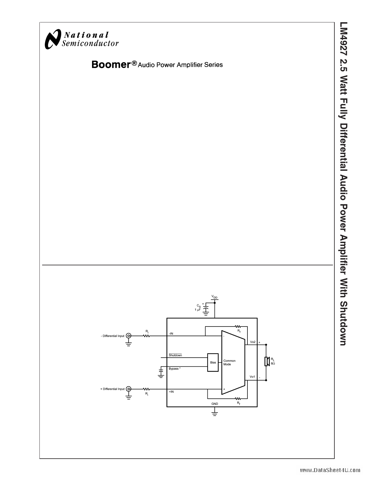
Typical Application
20152529
FIGURE 1. Typical Audio Amplifier Application Circuit
Boomer® is a registered trademark of National Semiconductor Corporation.
© 2006 National Semiconductor Corporation DS201525
www.national.com
1 page 
Typical Performance Characteristics (Note 10)
THD+N vs Frequency
VDD = 2.6V, RL = 8Ω, PO = 150mW
THD+N vs Frequency
VDD = 2.6V, RL = 4Ω, PO = 150mW
20152534
THD+N vs Frequency
VDD = 5V, RL = 8Ω, PO = 1W
20152533
THD+N vs Frequency
VDD = 5V, RL = 4Ω, PO = 1W
20152538
THD+N vs Frequency
VDD = 3V, RL = 8Ω, PO = 275mW
20152537
THD+N vs Frequency
VDD = 3V, RL = 4Ω, PO = 225mW
20152536
5
20152535
www.national.com
5 Page 
Application Information (Continued)
PDMAX = (VDD)2 / (2π2RL) Single-Ended
(2)
However, a direct consequence of the increased power de-
livered to the load by a bridge amplifier is an increase in
internal power dissipation versus a single-ended amplifier
operating at the same conditions.
PDMAX = 4 * (VDD)2 / (2π2RL) Bridge Mode
(3)
Since the LM4927 has bridged outputs, the maximum inter-
nal power dissipation is 4 times that of a single-ended am-
plifier. Even with this substantial increase in power dissipa-
tion, the LM4927 does not require additional heatsinking
under most operating conditions and output loading. From
Equation 3, assuming a 5V power supply and an 8Ω load,
the maximum power dissipation point is 625mW. The maxi-
mum power dissipation point obtained from Equation 3 must
not be greater than the power dissipation results from Equa-
tion 4:
PDMAX = (TJMAX - TA) / θJA
(4)
The LM4927’s θJA in an SDA08A package is 63˚C/W. De-
pending on the ambient temperature, TA, of the system
surroundings, Equation 4 can be used to find the maximum
internal power dissipation supported by the IC packaging. If
the result of Equation 3 is greater than that of Equation 4,
then either the supply voltage must be decreased, the load
impedance increased, the ambient temperature reduced, or
the θJA reduced with heatsinking. In many cases, larger
traces near the output, VDD, and GND pins can be used to
lower the θJA. The larger areas of copper provide a form of
heatsinking allowing higher power dissipation. For the typical
application of a 5V power supply, with an 8Ω load, the
maximum ambient temperature possible without violating the
maximum junction temperature is approximately 110˚C pro-
vided that device operation is around the maximum power
dissipation point. Recall that internal power dissipation is a
function of output power. If typical operation is not around the
maximum power dissipation point, the LM4927 can operate
at higher ambient temperatures. Refer to the Typical Per-
formance Characteristics curves for power dissipation in-
formation.
POWER SUPPLY BYPASSING
As with any power amplifier, proper supply bypassing is
critical for low noise performance and high power supply
rejection ratio (PSRR). The capacitor location on both the
bypass and power supply pins should be as close to the
device as possible. A larger half-supply bypass capacitor
improves PSRR because it increases half-supply stability.
Typical applications employ a 5V regulator with 10µF and
0.1µF bypass capacitors that increase supply stability. This,
however, does not eliminate the need for bypassing the
supply nodes of the LM4927. The LM4927 will operate with-
out the bypass capacitor CB, although the PSRR may de-
crease. A 1µF capacitor is recommended for CB. This value
maximizes PSRR performance. Lesser values may be used,
but PSRR decreases at frequencies below 1kHz. The issue
of CB selection is thus dependant upon desired PSRR and
click and pop performance as explained in the section
Proper Selection of External Components.
SHUTDOWN FUNCTION
In order to reduce power consumption while not in use, the
LM4927 contains shutdown circuitry that is used to turn off
the amplifier’s bias circuitry. The device may then be placed
into shutdown mode by toggling the Shutdown Select pin to
logic low. The trigger point for shutdown is shown as a typical
value in the Supply Current vs Shutdown Voltage graphs in
the Typical Performance Characteristics section. It is best
to switch between ground and supply for maximum perfor-
mance. While the device may be disabled with shutdown
voltages in between ground and supply, the idle current may
be greater than the typical value of 0.1µA. In either case, the
shutdown pin should be tied to a definite voltage to avoid
unwanted state changes.
In many applications, a microcontroller or microprocessor
output is used to control the shutdown circuitry, which pro-
vides a quick, smooth transition to shutdown. Another solu-
tion is to use a single-throw switch in conjunction with an
external pull-up resistor. This scheme guarantees that the
shutdown pin will not float, thus preventing unwanted state
changes.
PROPER SELECTION OF EXTERNAL COMPONENTS
Proper selection of external components in applications us-
ing integrated power amplifiers is critical when optimizing
device and system performance. Although the LM4927 is
tolerant to a variety of external component combinations,
consideration of component values must be made when
maximizing overall system quality.
The LM4927 is unity-gain stable, giving the designer maxi-
mum system flexibility. The LM4927 should be used in low
closed-loop gain configurations to minimize THD+N values
and maximize signal to noise ratio. Low gain configurations
require large input signals to obtain a given output power.
Input signals equal to or greater than 1Vrms are available
from sources such as audio codecs. Please refer to the
Audio Power Amplifier Design section for a more complete
explanation of proper gain selection. When used in its typical
application as a fully differential power amplifier the LM4927
does not require input coupling capacitors for input sources
with DC common-mode voltages of less than VDD. Exact
allowable input common-mode voltage levels are actually a
function of VDD, Ri, and Rf and may be determined by
Equation 5:
VCMi < (VDD-1.2)*((Rf+(Ri)/(Rf)-VDD*(Ri / 2Rf) (5)
-RF / RI = AVD
(6)
Special care must be taken to match the values of the input
resistors (Ri1 and Ri2) to each other. Because of the bal-
anced nature of differential amplifiers, resistor matching dif-
ferences can result in net DC currents across the load. This
DC current can increase power consumption, internal IC
power dissipation, reduce PSRR, and possibly damaging the
loudspeaker. The chart below demonstrates this problem by
showing the effects of differing values between the feedback
resistors while assuming that the input resistors are perfectly
matched. The results below apply to the application circuit
shown in Figure 1, and assumes that VDD = 5V, RL = 8Ω, and
the system has DC coupled inputs tied to ground.
11 www.national.com
11 Page | ||
| Páginas | Total 14 Páginas | |
| PDF Descargar | [ Datasheet LM4927.PDF ] | |
Hoja de datos destacado
| Número de pieza | Descripción | Fabricantes |
| LM4920 | Stereo Headphone Amplifier | National Semiconductor |
| LM49200 | Stereo Class AB Audio Subsystem with a True Ground Headphone Amplifier (Rev. A) | Texas Instruments |
| LM4921 | Low Voltage I2S 16-Bit Stereo DAC with Stereo Headphone Power Amplifiers and Volume Control | National Semiconductor |
| LM4921 | Low Voltage I 2 S 16-Bit Stereo DAC w/Stereo HP Pwr Amp Vol Cntrl (Rev. E) | Texas Instruments |
| Número de pieza | Descripción | Fabricantes |
| SLA6805M | High Voltage 3 phase Motor Driver IC. |
Sanken |
| SDC1742 | 12- and 14-Bit Hybrid Synchro / Resolver-to-Digital Converters. |
Analog Devices |
|
DataSheet.es es una pagina web que funciona como un repositorio de manuales o hoja de datos de muchos de los productos más populares, |
| DataSheet.es | 2020 | Privacy Policy | Contacto | Buscar |