|
|
|
PDF BUF16820 Data sheet ( Hoja de datos )
| Número de pieza | BUF16820 | |
| Descripción | 14-Channel GAMMA VOLTAGE GENERATOR | |
| Fabricantes | Burr-Brown | |
| Logotipo | ||
Hay una vista previa y un enlace de descarga de BUF16820 (archivo pdf) en la parte inferior de esta página. Total 30 Páginas | ||
|
No Preview Available !
BUF16820
BU F168 20
SBOS356A − FEBRUARY 2006 − REVISED OCTOBER 2006
14-Channel GAMMA VOLTAGE GENERATOR
with Programmable VCOM Outputs and OTP Memory
FEATURES
D 14-CHANNEL GAMMA CORRECTION
D 2 VCOM OUTPUTS
D ON-CHIP OTP MEMORY
D 10-BIT RESOLUTION
D RAIL-TO-RAIL OUTPUT
D LOW SUPPLY CURRENT: 1mA/ch
D SUPPLY VOLTAGE: 8.5V to 18V
D DIGITAL SUPPLY: 2.0V to 5.5V
D INDUSTRY-STANDARD, TWO-WIRE
INTERFACE: 3.4MHz HIGH-SPEED MODE
D HIGH ESD RATING:
4kV HBM, 1kV CDM, 200V MM
D DEMO BOARD AND SOFTWARE AVAILABLE
www.DataSheet4U.com
2V to 5.5V
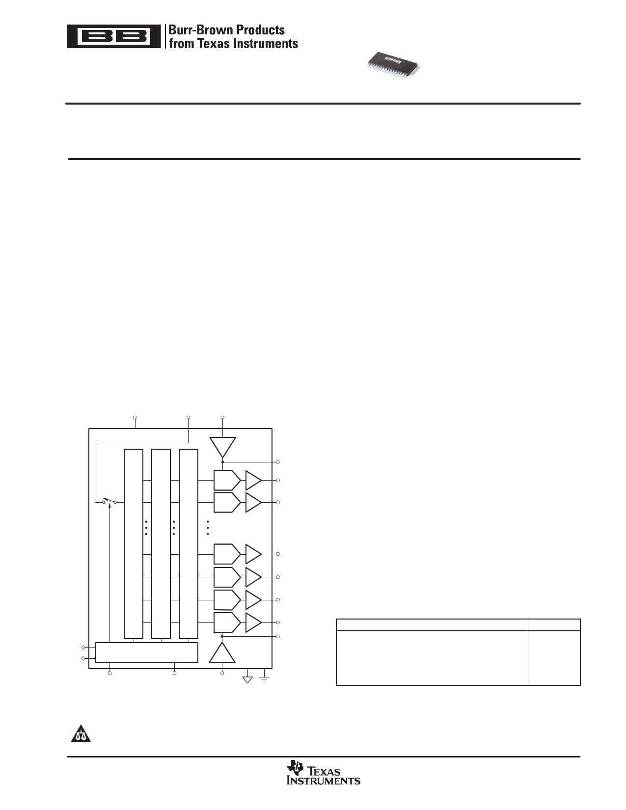
BUF16820
Digital
8.5V to 18V
Analog
REFH
SDA
SCL
Control IF
LD A0
REFH OUT
OUT1
OUT2
14 Output Channels plus
Two VCOM Channels
OUT13
OUT14
VCOM1
VCOM2
REFL OUT
REFL
APPLICATIONS
D REPLACES RESISTOR-BASED GAMMA
SOLUTIONS
D TFT-LCD REFERENCE DRIVERS
D DYNAMIC GAMMA CONTROL
DESCRIPTION
The BUF16820 is a programmable voltage reference
generator designed for gamma correction in TFT-LCD
panels. It provides 14 programmable outputs and two
VCOM channels, each with 10-bit resolution. It offers
on-chip, one-time programmable (OTP) memory that
allows the user to store the gamma voltages on-chip. This
eliminates the need for an external EEPROM.
This programmability replaces the traditional, time-
consuming process of changing resistor values to optimize
the various gamma voltages, and allows designers to
determine the correct gamma voltages for a panel very
quickly. Required voltage changes can also be easily
implemented without changing the hardware.
The BUF16820 uses TI’s latest, small-geometry analog
CMOS process, which makes it a very competitive choice
for full production, not just evaluation.
Programming of each output occurs through an industry-
standard, two-wire serial interface. Unlike existing
programmable buffers, the BUF16820 offers a high-speed
mode that allows clock speeds up to 3.4MHz.
For devices with a lower or higher channel count, please
contact your local sales or marketing representative.
The BUF16820 is available in an HTSSOP-32
PowerPAD package. It is specified from −40°C to +85°C.
BUF16820 RELATED PRODUCTS
FEATURES
18-Channel Programmable, Two VCOM Channels, Memory
12-Channel Programmable Buffer, 10-Bit
Programmable VCOM
10 + 1 Channel Gamma Buffer, 22V Supply Voltage
Complete LCD DC/DC Solution
PRODUCT
BUF20820
BUF12800
BUF01900
BUF11705
TPS651xx
Please be aware that an important notice concerning availability, standard warranty, and use in critical applications of Texas Instruments
semiconductor products and disclaimers thereto appears at the end of this data sheet.
PowerPAD is a registered trademark of Texas Instruments. All other trademarks are the property of their respective owners.
PRODUCTION DATA information is current as of publication date. Products
conform to specifications per the terms of Texas Instruments standard warranty.
Production processing does not necessarily include testing of all parameters.
Copyright 2006, Texas Instruments Incorporated
www.ti.com
1 page 
BUF16820
www.ti.com
APPLICATIONS INFORMATION
The BUF16820 programmable voltage reference allows
fast and easy adjustment of 14 programmable reference
outputs and two channels for VCOM adjustment, each with
10-bit resolution. It allows very simple, time-efficient
adjustment of the gamma reference and VCOM voltages.
The BUF16820 is programmed through a high-speed,
standard, two-wire interface. The BUF16820 features a
double-register structure for each DAC channel to simplify
the implementation of dynamic gamma control. This
structure allows pre-loading of register data and rapid
updating of all channels simultaneously.
Buffers 1−9 are able to swing to within 200mV of the
positive supply rail, and to within 0.6V of the negative
supply rail. Buffers 10−14 are able to swing to within 0.8V
of the positive supply rail and to within 200mV of the
negative supply rail.
The BUF16820 can be powered using an analog supply
voltage from 8.5V to 18V, and a digital supply from 2V to
5.5V. The digital supply must be applied prior to, or
simultaneously with, the analog supply to avoid excessive
current and power consumption; damage to the device
may occur if it is left connected only to the analog supply
for extended periods of time. Figure 7 shows the power
supply timing requirements.
Digital Supply:
VSD
GNDD
Analog Supply:
VS
GND
t1
t1: 0s minimum delay between Digital Supply and Analog Supply.
Figure 7. Power Supply Timing Requirements
Figure 8 shows the BUF16820 in a typical configuration.
In this configuration, the BUF16820 device address is 74h.
The output of each digital-to-analog converter (DAC) is
immediately updated as soon as data are received in the
corresponding register (LD = 0). For maximum dynamic
range, set VREFH = VS − 0.2V, and VREFL = GND + 0.2V.
TWO-WIRE BUS OVERVIEW
The BUF16820 communicates through an industry-
standard, two-wire interface to receive data in slave mode.
This standard uses a two-wire, open-drain interface that
supports multiple devices on a single bus. Bus lines are
driven to a logic low level only. The device that initiates the
SBOS356A − FEBRUARY 2006 − REVISED OCTOBER 2006
communication is called a master, and the devices
controlled by the master are slaves.The master generates
the serial clock on the clock signal line (SCL), controls the
bus access, and generates the START and STOP
conditions.
To address a specific device, the master initiates a START
condition by pulling the data signal line (SDA) from a HIGH
to a LOW logic level while SCL is HIGH. All slaves on the
bus shift in the slave address byte, with the last bit
indicating whether a read or write operation is intended.
During the 9th clock pulse, the slave being addressed
responds to the master by generating an acknowledge and
pulling SDA LOW.
Data transfer is then initiated and eight bits of data are sent
followed by an acknowledge bit. During data transfer, SDA
must remain stable while SCL is HIGH. Any change in
SDA while SCL is HIGH will be interpreted as a START or
STOP condition.
Once all data has been transferred, the master generates
a STOP condition indicated by pulling SDA from LOW to
HIGH while SCL is HIGH.
The BUF16820 can act only as a slave device; therefore,
it never drives SCL. The SCL pin is only an input for the
BUF16820. Table 1 and Table 2 summarize the address
and command codes, respectively, for the BUF16820.
Table 1. Quick-Reference Table of Addresses
DEVICE/COMPONENT
BUF16820 Address:
A0 pin is LOW
(device will acknowledge on address 74h)
A0 pin is HIGH
(device will acknowledge on address 75h)
ADDRESS
1110100
1110101
Table 2. Command Codes Quick-Reference
COMMAND
General Call Reset
High-Speed Mode
CODE
Address byte of 00h followed by a data byte
of 06h.
00001xxx, with SCL ≤ 400kHz; where xxx
are bits unique to the Hs-capable master.
This byte is called the Hs master code.
ADDRESSING THE BUF16820
The address of the BUF16820 is 111010x, where x is the
state of the A0 pin. When the A0 pin is LOW, the device will
acknowledge on address 74h (1110100). If the A0 pin is
HIGH, the device will acknowledge on address 75h
(1110101).
Other valid addresses are possible through a simple mask
change. Contact your TI representative for information.
5
5 Page 
www.ti.com
BUF16820
SBOS356A − FEBRUARY 2006 − REVISED OCTOBER 2006
a. Write Single DAC
b. Write Multiple DACs
Figure 9. Timing Diagram for Write DAC Register
11
11 Page | ||
| Páginas | Total 30 Páginas | |
| PDF Descargar | [ Datasheet BUF16820.PDF ] | |
Hoja de datos destacado
| Número de pieza | Descripción | Fabricantes |
| BUF16820 | 14-Channel GAMMA VOLTAGE GENERATOR | Burr-Brown |
| BUF16820 | 14-Channel Gamma Voltage Generator with Programmable Vcom Outputs and OTP Memory (Rev. B) | Texas Instruments |
| BUF16821 | Programmable Gamma-Volt Generator Vcom Calibrator w/Integrated 2-Bank Memory (Rev. C) | Texas Instruments |
| BUF16821-Q1 | BUF16821-Q1 Programmable Gamma-Voltage Generator and VCOM Calibrator with Integr | Texas Instruments |
| Número de pieza | Descripción | Fabricantes |
| SLA6805M | High Voltage 3 phase Motor Driver IC. |
Sanken |
| SDC1742 | 12- and 14-Bit Hybrid Synchro / Resolver-to-Digital Converters. |
Analog Devices |
|
DataSheet.es es una pagina web que funciona como un repositorio de manuales o hoja de datos de muchos de los productos más populares, |
| DataSheet.es | 2020 | Privacy Policy | Contacto | Buscar |