|
|
|
PDF W215B Data sheet ( Hoja de datos )
| Número de pieza | W215B | |
| Descripción | Notebook PC system Frequency Generator | |
| Fabricantes | Cypress Semiconductor | |
| Logotipo | ||
Hay una vista previa y un enlace de descarga de W215B (archivo pdf) en la parte inferior de esta página. Total 14 Páginas | ||
|
No Preview Available !
PRELIMINARY
W215B
Notebook PC System Frequency Generator for K6 Processors
Features
• Generates system clocks for CPU, IOAPIC, SDRAM,
PCI, USB plus 14.318 MHz (REF0:1)
• MODE input pin selects optional power management
input control pins (reconfigures pins 26 and 27)
• Two fixed outputs separately selectable as 24-MHz or
48-MHz (default = 48-MHz)
• VDDQ3 = 3.3V±5%, VDDQ2 = 3.3V±5%
• Uses external 14.318-MHz crystal
• Available in 48-pin TSSOP (6.1-mm)
• 10Ω CPU output impedance
Table 1. Pin Selectable Frequency
95/100_SEL
CPU, SDRAM
Clocks (MHz)
0 95.0
1 100.0
PCI Clocks
CPU/3
CPU/3
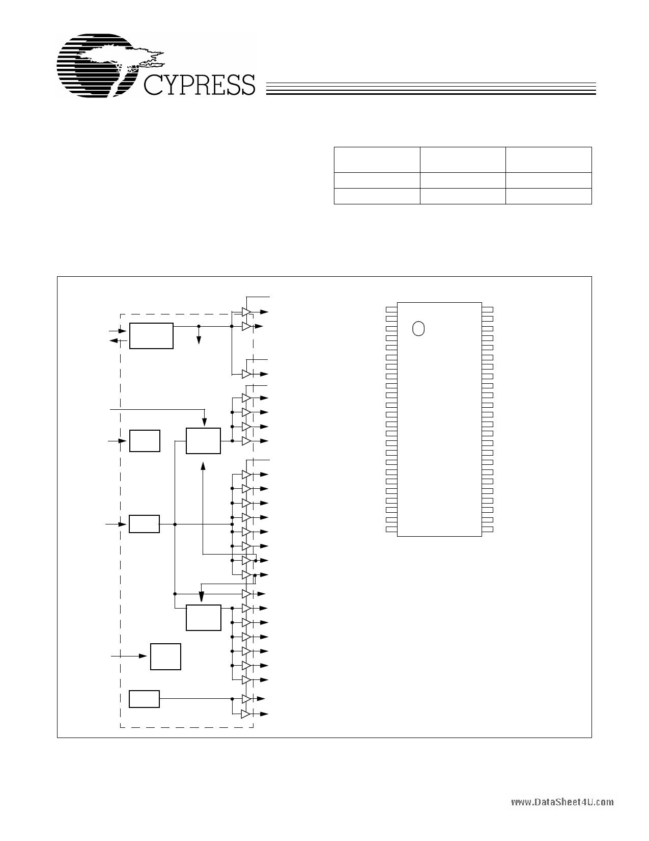
Block Diagram
X1 XTAL
X2 OSC
PLL Ref Freq
www.DataSheet4U.com
CPU_2.5#
MODE
I/O
Control
Stop
Output
Control
95/100_SEL
PLL 1
PWR_DWN#
Stop
Output
Control
Power
Down
Control
PLL2
VDDQ3
REF0
REF1
VDDQ2
IOAPIC
VDDQ2
CPU0
CPU1
CPU2
CPU3
VDDQ3
SDRAM0
SDRAM1
SDRAM2
SDRAM3
SDRAM4
Pin Configuration
REF1
REF0
GND
X1
X2
MODE
VDDQ3
PCI_F
PCI0
GND
PCI1
PCI2
PCI3
PCI4
VDDQ3
PCI5
GND
95/100_SEL
Reserved
Reserved
VDDQ3
48/24MHZ
48/24MHZ
GND
1
2
3
4
5
6
7
8
9
10
11
12
13
14
15
16
17
18
19
20
21
22
23
24
SDRAM5
SDRAM6/CPUSTOP#
SDRAM7/PCISTOP#
PCI_F
PCI0
PCI1
PCI2
PCI3
PCI4
PCI5
48/24MHZ
48/24MHZ
48 VDDQ3
47 CPU_2.5#
46 VDDQ2
45 IOAPIC
44 PWR_DWN#
43 GND
42 CPU0
41 CPU1
40 VDDQ2
39 CPU2
38 CPU3
37 GND
36 SDRAM0
35 SDRAM1
34 VDDQ3
33 SDRAM2
32 SDRAM3
31 GND
30 SDRAM4
29 SDRAM5
28 VDDQ3
27 SDRAM6/CPU_STOP#
26 SDRAM7/PCI_STOP#
25 VDDQ3
Cypress Semiconductor Corporation • 3901 North First Street • San Jose • CA 95134 • 408-943-2600
Document #: 38-07222 Rev. *A*
Revised December 15, 2002
1 page 
PRELIMINARY
W215B
DC Electrical Characteristics (continued)
TA = 0°C to +70°C, VDDQ3 = 3.3V±5% (3.135–3.465V), fXTL = 14.31818 MHz, VDDQ2 = 3.3V±5%
Parameter
Description
Test Condition
Min. Typ. Max. Unit
Crystal Oscillator
VTH X1 Input Threshold Voltage[4]
CLOAD
Load Capacitance, Imposed on External
Crystal[5]
CIN,X1
X1 Input Capacitance[6]
Pin Capacitance/Inductance
VDDQ3 = 3.3V
Pin X2 unconnected
1.65 V
14 pF
28 pF
CIN Input Pin Capacitance
Except X1 and X2
5 pF
COUT
Output Pin Capacitance
6 pF
LIN Input Pin Inductance
7 nH
Notes:
4. X1 input threshold voltage (typical) is VDDQ3/2.
5. The W215B contains an internal crystal load capacitor between pin X1 and ground and another between pin X2 and ground. Total load placed on crystal is
14 pF; this includes typical stray capacitance of short PCB traces to crystal.
6. X1 input capacitance is applicable when driving X1 with an external clock source (X2 is left unconnected).
AC Electrical Characteristics (Lump Load Model)
TA = 0°C to +70°C, VDDQ3 = 3.3V±5% (3.135–3.465V) fXTL = 14.31818 MHz, VDDQ2 = 3.3V±5%
AC clock parameters are tested and guaranteed over stated operating conditions using the stated lump capacitive load at the
clock output.
www.DataSheet4U.com
Test Point
FTG
*20pF for CPU, REF1, IOAPIC,
24MHz & 48MHz
*30pF for SDRAM & PCI
CPU Clock Outputs, CPU0:3 (Lump Capacitance Test Load = 20 pF)
Parameter
tP
f
tH
tL
tR
tF
tD
tJC
tSK
fST
Zo
Description
Period
Frequency, Actual
High Time
Low Time
Output Rise Edge Rate
Output Fall Edge Rate
Duty Cycle
Jitter, Cycle-to-Cycle
Output Skew
Frequency Stabilization from
Power-up (cold start)
AC Output Impedance
Test Condition/Comments
Measured on rising edge at 1.5V
Determined by PLL divider ratio
Duration of clock cycle above 2.4V
Duration of clock cycle below 0.4V
Measured from 0.4V to 2.4V
Measured from 2.4V to 0.4V
Measured on rising and falling edge at 1.5V
Measured on rising edge at 1.5V. Maximum differ-
ence of cycle time between two adjacent cycles.
Measured on rising edge at 1.5V
Assumes full supply voltage reached within 1 ms
from power-up. Short cycles exist prior to frequency
stabilization.
Average value during switching transition. Used for
determining series termination value.
CPU = 100 MHz
Min. Typ. Max.
10
100
5
5
14
14
45 50 55
500
250
3
10
Unit
ns
MHz
ns
ns
V/ns
V/ns
%
ps
ps
ms
Ω
Document #: 38-07222 Rev. *A*
Page 5 of 14
5 Page 
PRELIMINARY
W215B
48-/24-MHz Clock Output (Test Load: R = 33Ω; C = 22 pF)
Parameter
Description
m/n PLL Ratio
tR Output Rise Edge Rate
tF Output Fall Edge Rate
tD Duty Cycle
fST Frequency Stabilization
from Power-up (cold start)
Zo AC Output Impedance
Test Condition/Comments
Measured on rising and falling edge at 1.5V
Assumes full supply voltage reached within 1 ms
from power-up. Short cycles exist prior to fre-
quency stabilization.
Average value during switching transition. Used
for determining series termination value.
CPU = 100 MHz
Min. Typ. Max.
57/17
0.5 2
0.5 2
45 50 55
3
25
Unit
V/ns
V/ns
%
ms
Ω
Ordering Information
Ordering Code
Package
Name
W215B
X
Package Type
48-pin TSSOP (6.1 mm)
www.DataSheet4U.com
Document #: 38-07222 Rev. *A*
Page 11 of 14
11 Page | ||
| Páginas | Total 14 Páginas | |
| PDF Descargar | [ Datasheet W215B.PDF ] | |
Hoja de datos destacado
| Número de pieza | Descripción | Fabricantes |
| W215 | Vitreous Enamelled Wirewound Resistors | ETC |
| W2152 | A Major Advance | ETC |
| W215B | Notebook PC system Frequency Generator | Cypress Semiconductor |
| Número de pieza | Descripción | Fabricantes |
| SLA6805M | High Voltage 3 phase Motor Driver IC. |
Sanken |
| SDC1742 | 12- and 14-Bit Hybrid Synchro / Resolver-to-Digital Converters. |
Analog Devices |
|
DataSheet.es es una pagina web que funciona como un repositorio de manuales o hoja de datos de muchos de los productos más populares, |
| DataSheet.es | 2020 | Privacy Policy | Contacto | Buscar |