|
|
|
PDF 33882 Data sheet ( Hoja de datos )
| Número de pieza | 33882 | |
| Descripción | Six-Output Low-Side Switch | |
| Fabricantes | Freescale Semiconductor | |
| Logotipo | ||
Hay una vista previa y un enlace de descarga de 33882 (archivo pdf) en la parte inferior de esta página. Total 27 Páginas | ||
|
No Preview Available !
www.DFaretaeSshceeatl4eUS.ceommiconductor
Advance Information
Document Number: MC33882
Rev. 5.0, 10/2006
Six-Output Low-Side Switch
with SPI and Parallel Input
Control
33882
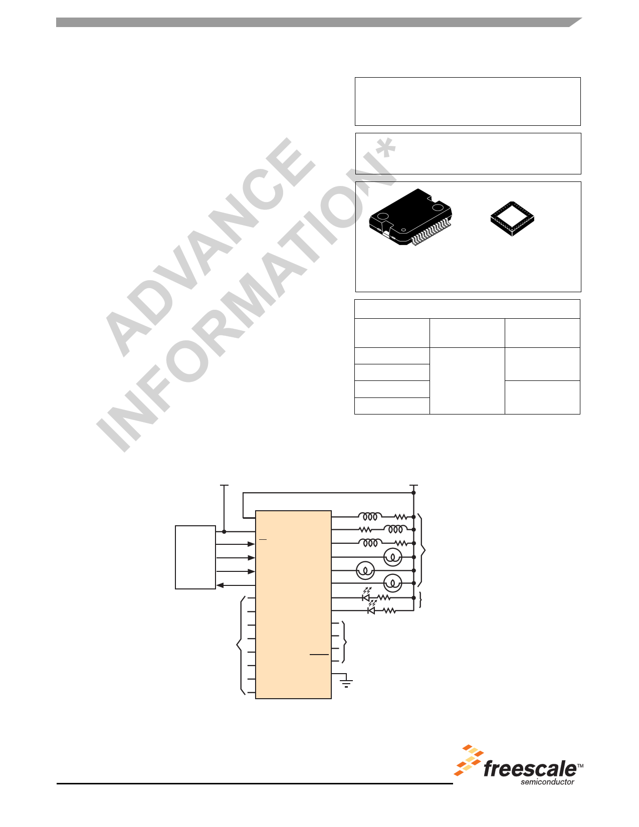
The 33882 is a smart six-output low-side switch able to control
system loads up to 1.0 A. The six outputs can be controlled via both
serial peripheral interface (SPI) and parallel input control, making the
device attractive for fault-tolerant system applications. There are two
additional 30 mA low-side switches with SPI diagnostic reporting
(with parallel input control only).
The 33882 is designed to interface directly with industry-standard
microcontrollers via SPI to control both inductive and incandescent
loads. Outputs are configured as open-drain power MOSFETs
incorporating internal dynamic clamping and current limiting. The
device has multiple monitoring and protection features, including low
standby current, fault status reporting, internal 52 V clamp on each
output, output-specific diagnostics, and protective shutdown. In
addition, it has a mode select pin affording a dual means of input
control.
Features
• Outputs Clamped for Switching Inductive Loads
• Very Low Operational Bias Currents (< 2.0 mA)
• CMOS Input Logic Compatible with 5.0 V Logic Levels
• Load Dump Robust (60 V Transient at VPWR on OUT0–OUT5)
• Daisy Chain Operation of Multiple Devices Possible
• Switch Outputs Can Be Paralleled for Higher Currents
• RDS(ON) of 0.4 Ω per Output (25°C) at 13 V VPWR
• SPI Operation Guaranteed to 2.0 MHz
• Pb-Free Packaging Designated by Suffix Codes VW and EP
SIX-OUTPUT LOW-SIDE SWITCH
DH SUFFIX
VW SUFFIX (PB-FREE)
98ASH70329A
30-PIN HSOP
FC SUFFIX
EP SUFFIX (PB-FREE)
98ARH99032A
32-PIN QFN
ORDERING INFORMATION
Device
Temperature
Range (TA)
Package
MC33882DH/R2
MC33882VW/R2
MC33882FC/R2
MC33882EP/R2
-40°C to 125°C
30 HSOP
32 QFN
VDD VPWR
MCU
Optional Parallel
Control of
Outputs 0 through 7
33882
VPWR
VDD
CS
SCLK
SI
SO
IN0
IN1
IN2
IN3
IN4
IN5
IN6
OUT0
OUT1
OUT2
OUT3
OUT4
OUT5
OUT6
OUT7
IN0 & IN1
IN2 & IN3
IN4 & IN5
MODE
GND
IN7
Optional Control
of Paired Outputs
High-Power
Outputs
Low-Power
LED
Outputs
Figure 1. 33882 Simplified Application Diagram
* This document contains certain information on a new product.
Specifications and information herein are subject to change without notice.
© Freescale Semiconductor, Inc., 2006. All rights reserved.
1 page 
PIN CONNECTIONS
Transparent Top View of Package
IN4 & IN5
IN6
OUT6
GND
GND
VPWR
IN0 & IN1
MODE
1
2
3
4
5
6
7
8
24 OUT7
23
VDD
22
GND
21
GND
20
GND
19
GND
18
SO
17
CS
Figure 4. QFN Pin Connections
Table 2. QFN Pin Function Description
Pin
Pin Name
Formal Name
7
IN0 & IN1
Input 0 & Input 1
26
IN2 & IN3
Input 2 & Input 3
1
IN4 & IN5
Input 4 & Input 5
2
9
11
13
25
28
30
32
3
10
12
14
24
27
29
31
4, 5, 19–22
6
8
15
IN6
IN0
IN1
IN2
IN7
IN3
IN4
IN5
OUT6
OUT0
OUT1
OUT2
OUT7
OUT3
OUT4
OUT5
GND
VPWR
MODE
SI
Input 0–Input 7
Output 0–Output 7
Ground
Load Supply Voltage
Mode Select
Serial Input
Definition
These input pins control two output channels each when the MODE pin is pulled high.
These pins may be connected to pulse width modulated (PWM) outputs of the control
IC while the MODE pin is high. The states of these pins are ignored during normal
operation (MODE pin low) and override the normal inputs (serial or parallel) when the
MODE pin is high. These pins have internal active 25 µA pull-downs.
These are parallel input pins. These pins have internal 25 µA active pull-downs.
Each pin is one channel's drain, sinking current for the respective load.
Ground continuity is required for the outputs to turn on.
This pin is connected to battery voltage. A decoupling capacitor is required from
VPWR to ground.
The MODE pin is connected to the MODE pin of the control IC. This pin has an internal
active 25 µA pull-up.
The Serial Input pin is connected to the SPI Serial Data Output pin of the control IC
from where it receives output command data. This input has an internal active 25 µA
pull-down and requires CMOS logic levels.
Analog Integrated Circuit Device Data
Freescale Semiconductor
33882
5
5 Page 
ELECTRICAL CHARACTERISTICS
DYNAMIC ELECTRICAL CHARACTERISTICS
DYNAMIC ELECTRICAL CHARACTERISTICS
Table 5. Dynamic Electrical Characteristics
Characteristics noted under conditions 4.75 V ≤ VDD ≤ 5.25 V, 9.0 V ≤ VPWR ≤ 17 V, -40°C ≤ TA ≤ 125°C unless otherwise
noted.
Characteristic
Symbol
Min
Typ
Max Unit
POWER OUTPUT TIMING
Output Rise Time (27)
Output Fall Time (27)
Output Turn-ON Delay Time (28)
Output Turn-OFF Delay Time (29)
Output Short Fault Sense Time (30)
RLOAD = < 1.0 V
Output Short Fault Refresh Time (31)
RLOAD = < 1.0 V
Output OFF Open Load Sense Time (32)
Output ON Open Load Sense Time (33)
Output Short Fault ON Duty Cycle (34)
DIGITAL INTERFACE TIMING
SCLK Clock High Time (SCLK = 3.2 MHz) (35)
SCLK Clock Low Time (SCLK = 3.2 MHz) (35)
Falling Edge (0.8 V) of CS to Rising Edge (2.0 V) of SCLK
Required Setup Time (35)
tR 1.0 – 10 µs
tF 1.0 – 10 µs
tDLY (ON)
1.0
–
10 µs
tDLY (OFF)
1.0
–
10 µs
tSS µs
25 – 100
t REF
ms
3.0 4.5 6.0
t OS(OFF)
25
60 100 µs
t OS(ON)
3.0
–
12 ms
SC DC
0.42
–
3.22 %
t SCLKH
t SCLKL
t LEAD
–
–
–
– 141 ns
– 141 ns
ns
– 140
Falling Edge (0.8 V) of SCLK to Rising Edge (2.0 V) of CS
Required Setup Time (35)
t LAG
–
ns
– 50
SI, CS, SCLK Incoming Signal Rise Time (35)
SI, CS, SCLK Incoming Signal Fall Time (35)
t RSI
t FSI
–
–
– 50 ns
– 50 ns
Notes
27. Output Rise and Fall time measured at 10% to 90% and 90% to 10% voltage points respectively across 15 Ω resistive load to a VBAT
of 15 V, VPWR = 15 V.
28. Output Turn-ON Delay Time measured from rising edge (3.0 V) VIN (CS for serial) to 90% VO using a 15 Ω load to a VBAT of 15 V,
VPWR = 15 V.
29. Output Turn-OFF Delay Time measured from falling edge (1.0 V) VIN (3.0 V rising edge of CS for serial) to 10% VO using a 15 Ω load
to a VBAT of 15 V, VPWR = 15 V.
30. The shorted output is turned ON during tSS to retry and check if the short has cleared. The shorted output is in current limit during tSS.
The tSS is measured from the start of current limit to the end of current limit.
31. The Short Fault Refresh Time is the waiting period between tSS retry signals. The shorted output is disabled during this refresh time.
The tREF is measured from the end of current limit to the start of current limit.
32. The tOS(OFF) is measured from the time the faulted output is turned OFF until the fault bit is available to be loaded into the internal fault
register. To guarantee a fault is reported on SO, the falling edge of CS must occur at least 100 µs after the faulted output is off.
33. The tOS(ON) is measured from the time the faulted output is turned ON until the fault bit is available to be loaded into the internal fault
register. To guarantee a fault is reported on SO, the falling edge of CS must occur at least 12 ms after the faulted output is ON.
34. Percent Output Short Fault ON Duty Cycle is defined as (tSS) ÷ (tREF) x 100. This specification item is provided FYI and is not tested.
35. Parameter is not tested and values suggested are for system design consideration only in preventing the occurrence of double pulsing.
Analog Integrated Circuit Device Data
Freescale Semiconductor
33882
11
11 Page | ||
| Páginas | Total 27 Páginas | |
| PDF Descargar | [ Datasheet 33882.PDF ] | |
Hoja de datos destacado
| Número de pieza | Descripción | Fabricantes |
| 33880 | Configurable Octal Serial Switch | Freescale Semiconductor |
| 33882 | Six-Output Low-Side Switch | Freescale Semiconductor |
| 33883 | H-Bridge Gate Driver IC | Freescale Semiconductor |
| 33884 | Switch Monitor Interface | Freescale Semiconductor |
| Número de pieza | Descripción | Fabricantes |
| SLA6805M | High Voltage 3 phase Motor Driver IC. |
Sanken |
| SDC1742 | 12- and 14-Bit Hybrid Synchro / Resolver-to-Digital Converters. |
Analog Devices |
|
DataSheet.es es una pagina web que funciona como un repositorio de manuales o hoja de datos de muchos de los productos más populares, |
| DataSheet.es | 2020 | Privacy Policy | Contacto | Buscar |