|
|
|
PDF 33886 Data sheet ( Hoja de datos )
| Número de pieza | 33886 | |
| Descripción | 5.0 A H-Bridge | |
| Fabricantes | Freescale Semiconductor | |
| Logotipo | ||
Hay una vista previa y un enlace de descarga de 33886 (archivo pdf) en la parte inferior de esta página. Total 25 Páginas | ||
|
No Preview Available !
www.DFaretaeSshceeatl4eUS.ceommiconductor
Technical Data
5.0 A H-Bridge
The 33886 is a monolithic H-Bridge ideal for fractional horsepower
DC-motor and bi-directional thrust solenoid control. The IC
incorporates internal control logic, charge pump, gate drive, and low
RDS(ON) MOSFET output circuitry. The 33886 is able to control
continuous inductive DC load currents up to 5.0 A. Output loads can
be pulse width modulated (PWM-ed) at frequencies up to 10 kHz.
A Fault Status output reports undervoltage, short circuit, and
overtemperature conditions. Two independent inputs control the two
half-bridge totem-pole outputs. Two disable inputs force the H-Bridge
outputs to tri-state (exhibit high impedance).
The 33886 is parametrically specified over a temperature range of
-40°C ≤ TA ≤ 125°C, 5.0 V ≤ V+ ≤ 28 V. The IC can also be operated
up to 40 V with derating of the specifications. The IC is available in a
surface mount power package with exposed pad for heatsinking.
Features
• 5.0 V to 40 V Continuous Operation
• 120 mΩ RDS(ON) H-Bridge MOSFETs
• TTL /CMOS Compatible Inputs
• PWM Frequencies up to 10 kHz
• Active Current Limiting via Internal Constant OFF-Time PWM (with
Temperature-Dependent Threshold Reduction)
• Output Short Circuit Protection
• Undervoltage Shutdown
• Fault Status Reporting
• Pb-Free Packaging Designated by Suffix Code VW
Document Number: MC33886
Rev 8.0, 2/2007
33886
H-BRIDGE
VW SUFFIX (PB-FREE)
DH SUFFIX
98ASH70702A
20-PIN HSOP
ORDERING INFORMATION
Device
Temperature
Range (TA)
Package
MC33886DH/R2
MC33886VW/R2
-40°C to 125°C
20 HSOP
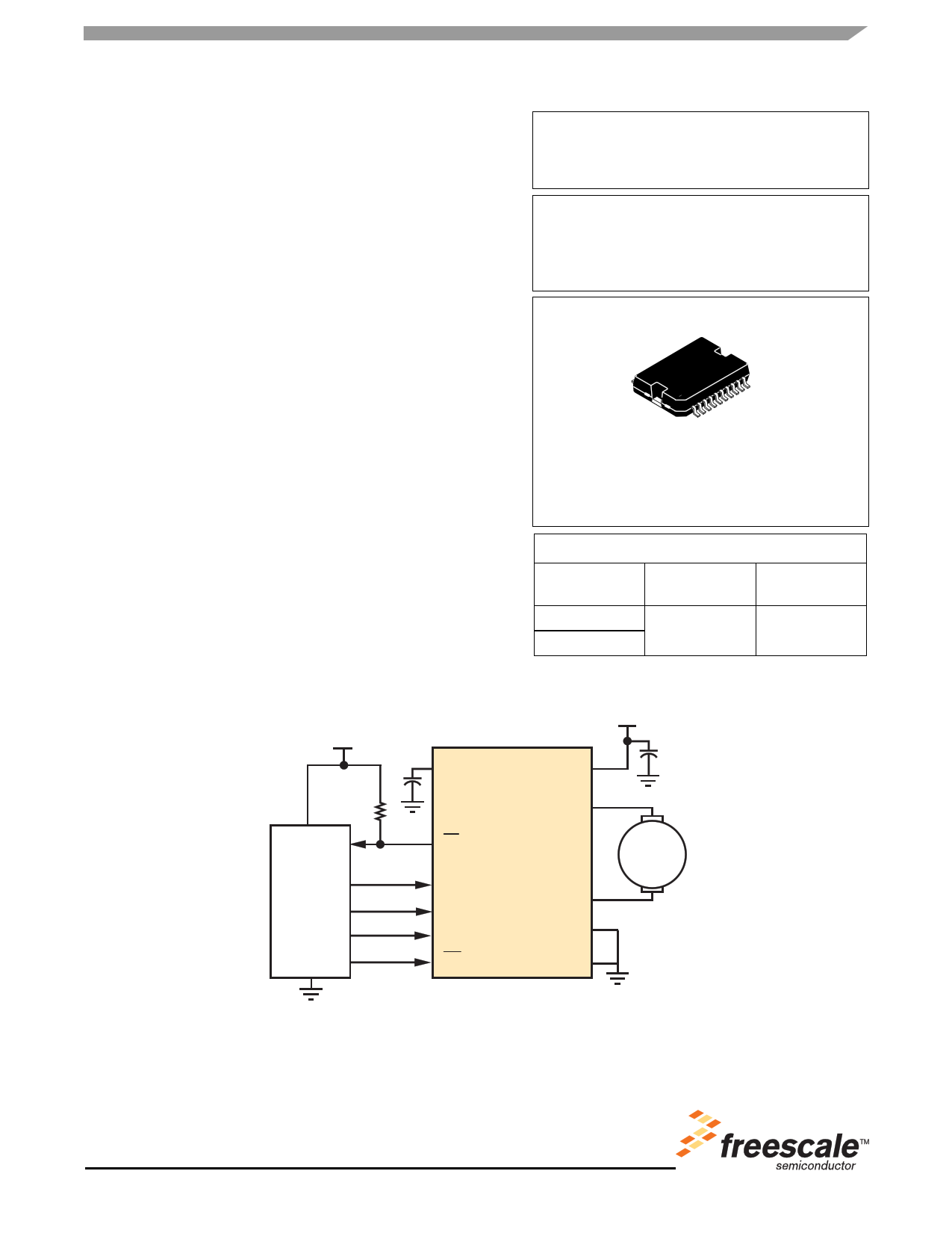
5.0 V
IN
OUT
MCU
OUT
OUT
OUT
33886
CCP
V+
OUT1
FS
IN1
OUT2
IN2
D1 PGND
D2 AGND
V+
MOTOR
Figure 1. 33886 Simplified Application Diagram
Freescale Semiconductor, Inc. reserves the right to change the detail specifications,
as may be required, to permit improvements in the design of its products.
© Freescale Semiconductor, Inc., 2007. All rights reserved.
1 page 
ELECTRICAL CHARACTERISTICS
STATIC ELECTRICAL CHARACTERISTICS
STATIC ELECTRICAL CHARACTERISTICS
Table 3. Static Electrical Characteristics
Characteristics noted under conditions 5.0 V ≤ V+ ≤ 28 V and -40°C ≤ TA ≤ 125°C unless otherwise noted. Typical values noted
reflect the approximate parameter mean at TA = 25°C under nominal conditions unless otherwise noted.
Characteristic
Symbol
Min Typ Max Unit
POWER SUPPLY
Operating Voltage Range (11)
V+
5.0 –
40 V
Standby Supply Current
VEN = 5.0 V, IOUT = 0 A
IQ (standby)
mA
– – 20
Threshold Supply Voltage
Switch-OFF
Switch-ON
Hysteresis
CHARGE PUMP
V+(thres-OFF)
V+(thres-ON)
V+(hys)
4.15
4.5
150
4.4
4.75
–
4.65 V
5.0 V
– mV
Charge Pump Voltage
V+ = 5.0 V
8.0 V ≤ V+ ≤ 40 V
VCP - V+
3.35 –
––
V
–
20
CONTROL INPUTS
Input Voltage (IN1, IN2, D1, D2)
Threshold High
Threshold Low
Hysteresis
Input Current (IN1, IN2, D1) (12)
VIN = 0 V
D2 Input Current (13)
V D2 = 5.0 V
VIH
VIL
VHYS
IIN
I D2
3.5
–
0.7
-200
–
–
–
1.0
-80
25
V
–
1.4
–
µA
–
µA
100
Notes
11. Specifications are characterized over the range of 5.0 V ≤ V+ ≤ 28 V. Operation >28 V will cause some parameters to exceed listed
min/max values. Refer to typical operating curves to extrapolate values for operation >28 V but ≤ 40 V.
12. Inputs IN1, IN2, and D1 have independent internal pull-up current sources.
13. The D2 input incorporates an active internal pull-down current sink.
Analog Integrated Circuit Device Data
Freescale Semiconductor
33886
5
5 Page 
TYPICAL SWITCHING WAVEFORMS
Output Voltage
(OUT1)
Output Voltage
(OUT1)
IOUT
Input Voltage
(IN1)
V+=24 V
fPWM=10 kHz Duty Cycle=50%
IOUT
Input Voltage
(IN1)
V+=12 V
fPWM=20 kHz Duty Cycle=50%
Figure 14. Output Voltage and Current vs. Input Voltage
at V+ = 24 V, PMW Frequency of 10 kHz,
and Duty Cycle of 50%
Figure 16. Output Voltage and Current vs. Input Voltage
at V+ = 12 V, PMW Frequency of 20 kHz,
and Duty Cycle of 50% for a Purely Resistive Load
Output Voltage
(OUT1)
Output Voltage
(OUT1)
IOUT
IOUT
Input Voltage
(IN1)
V+=24 V
fPWM=10 kHz Duty Cycle=90%
Input Voltage
(IN1)
V+=12 V
fPWM=20 kHz Duty Cycle=90%
Figure 15. Output Voltage and Current vs. Input Voltage
at V+ = 24 V, PMW Frequency of 10 kHz,
and Duty Cycle of 90%
Figure 17. Output Voltage and Current vs. Input Voltage
at V+ = 12 V, PMW Frequency of 20 kHz,
and Duty Cycle of 90% for a Purely Resistive Load
Analog Integrated Circuit Device Data
Freescale Semiconductor
33886
11
11 Page | ||
| Páginas | Total 25 Páginas | |
| PDF Descargar | [ Datasheet 33886.PDF ] | |
Hoja de datos destacado
| Número de pieza | Descripción | Fabricantes |
| 33880 | Configurable Octal Serial Switch | Freescale Semiconductor |
| 33882 | Six-Output Low-Side Switch | Freescale Semiconductor |
| 33883 | H-Bridge Gate Driver IC | Freescale Semiconductor |
| 33884 | Switch Monitor Interface | Freescale Semiconductor |
| Número de pieza | Descripción | Fabricantes |
| SLA6805M | High Voltage 3 phase Motor Driver IC. |
Sanken |
| SDC1742 | 12- and 14-Bit Hybrid Synchro / Resolver-to-Digital Converters. |
Analog Devices |
|
DataSheet.es es una pagina web que funciona como un repositorio de manuales o hoja de datos de muchos de los productos más populares, |
| DataSheet.es | 2020 | Privacy Policy | Contacto | Buscar |