|
|
|
PDF R2J20701NP Data sheet ( Hoja de datos )
| Número de pieza | R2J20701NP | |
| Descripción | Peak Current Mode Synchronous Buck Controller | |
| Fabricantes | Renesas Technology | |
| Logotipo | ||
Hay una vista previa y un enlace de descarga de R2J20701NP (archivo pdf) en la parte inferior de esta página. Total 28 Páginas | ||
|
No Preview Available !
www.DataSheet4U.com
R2J20701NP
Peak Current Mode Synchronous Buck Controller
with Power MOS FETs
REJ03G1459-0300
Rev.3.00
Jun 20, 2007
Description
This all-in-one SiP for POL (point-of-load) applications is a multi-chip module incorporating a high-side MOS FET,
low-side MOS FET, and PWM controller in a single QFN package. The on and off timing of the power MOS FET is
optimized by the built-in driver circuit, making this device suitable for large-current high-efficiency buck converters.
In a simple peak-current mode topology, stable operation is obtained in a closed power loop, and a fast converter is
easily realized with the addition of simple components. Furthermore, the same topology can be applied to realize
converters for parallel synchronized operation with current sharing, and two-phase operation.
The package also incorporates a high-side bootstrap Schottky barrier diode (SBD), eliminating the need for an external
SBD for this purpose.
Features
• Three chips in one package for high-efficiency and space saving
• Large average output current (35 A)
• Wide input voltage range: 8 to 14 V
• 0.6 V reference voltage accurate to within 1%
• Wide programmable switching frequency: 200 kHz to 1 MHz
• Fast response by peak-current-mode topology.
• Simple current sharing (up to five modules in parallel)
• Two-phase operation in parallel operation
• Built-in SBD for boot strapping
• On/off control
• Hiccup operation under over load condition
• Tracking function
• Thin small package: 56-pin QFN (8 mm × 8 mm)
Applications
• Network equipment
• Telecommunications equipment
• Servers
• POL modules
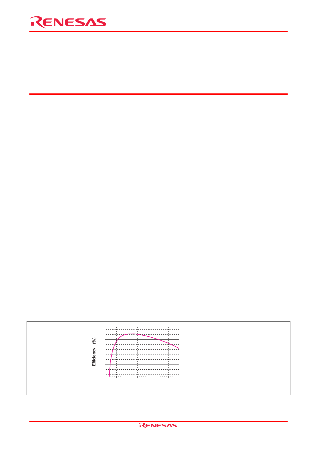
Typical Characteristic Curve
95
90
VIN = 12 V
VOUT = 1.8 V
85 L = 440 nH
CO = 600 µF
80 Frequency = 500 kHz
No airflow
Ta = 27°C
75
0 5 10 15 20 25 30 35
Iout (A)
REJ03G1459-0300 Rev.3.00 Jun 20, 2007
Page 1 of 27
1 page 
R2J20701NP
Pin Description
Pin Name
VIN
SW
PGND
Pin No.
10 to 20
9, 21, 40 to 48
22 to 39
Description
Input voltage for the buck converter.
Switching node. Connect a choke coil between the
SW pin and dc output node of the converter.
Ground of the power stage.
SGND
6, 52
Ground of the IC chip.
VCIN
BOOT
REG5
7 Input voltage for the control circuit.
8 Bootstrap voltage pin. A bootstrap capacitor should
be connected between the BOOT and SW pin.
5 +5 V logic power-supply output.
ON/OFF
50 Signal disable pin.
IREF
4 Reference current generator for the IC.
CT
SYNC
TRK-SS
FB
EO
55 Timing capacitor pin for the oscillator. This pin has a
select function for operation in slave mode.
49 I/O pin for synchronous operation.
56 Start-up timing control input.
1 Feedback voltage input for the closed loop.
3 Error amplifier output pin.
Ishare
2 For current-sharing bus.
RAMP
CS
54 RAMP signal input pin for peak current mode PWM
control.
53 Current output pin of active current sensing circuit.
DRV5
51 +5.25 V generator output for driving power MOS
FETs.
Remarks
Should be externally connected to
SGND.
Should be externally connected to
PGND.
Should be externally connected to VIN.
To be supplied +5 V through the
internal SBD.
Requires decoupling from the GND
plane by a capacitance 0.1 µF.
Disabled when ON/OFF pin is in the
low state.
Should be connected via 27 kΩ to the
SGND pin.
If the pin voltage is <1 V or >4 V, the IC
operates in slave mode.
Requires connection to an RC circuit
for loop compensation.
Simply connect the Ishare pins of all
devices to get balanced current.
Appropriate resistance is required
between CS and the GND plane.
Requires decoupling from the GND
plane by a capacitance from 0.1 µF to
1.0 µF.
REJ03G1459-0300 Rev.3.00 Jun 20, 2007
Page 5 of 27
5 Page 
R2J20701NP
Application Example
Start-up Settings
Case 1) Standalone or master chip in parallel operation
With the RC network on the TRK-SS pin, the voltage on the pin should ramp up slowly.
R REG5
TRK-SS
C
ON/OFF
TRK-SS
Vout
0.6 V
TSS = − CR × Ln (1 − 0.6 V / 5 V) (s)
Case 2)
Coincident tracking
The TRS-SS signal for channel two is the voltage from Vout1 after division by a resistor network. Vout1
must be greater than Vout2. Cross-talk is not generated between the channels.
R REG5
Channel 1
TRK-SS
SW
C
FB
From Vout1
R3 REG5
Channel 2
TRK-SS
SW
R4 FB
Vout1
R1
Vout1 (nominal) = 0.6 V × (R1 + R2) / R2
R2
Vout2
R3
Vout2 (nominal) = 0.6 V × (R3 + R4) / R4
R4
Output
voltage
Vout1
Vout2
Time
REJ03G1459-0300 Rev.3.00 Jun 20, 2007
Page 11 of 27
11 Page | ||
| Páginas | Total 28 Páginas | |
| PDF Descargar | [ Datasheet R2J20701NP.PDF ] | |
Hoja de datos destacado
| Número de pieza | Descripción | Fabricantes |
| R2J20701NP | Peak Current Mode Synchronous Buck Controller | Renesas Technology |
| Número de pieza | Descripción | Fabricantes |
| SLA6805M | High Voltage 3 phase Motor Driver IC. |
Sanken |
| SDC1742 | 12- and 14-Bit Hybrid Synchro / Resolver-to-Digital Converters. |
Analog Devices |
|
DataSheet.es es una pagina web que funciona como un repositorio de manuales o hoja de datos de muchos de los productos más populares, |
| DataSheet.es | 2020 | Privacy Policy | Contacto | Buscar |