|
|
|
PDF G2U09N70 Data sheet ( Hoja de datos )
| Número de pieza | G2U09N70 | |
| Descripción | N-CHANNEL ENHANCEMENT MODE POWER MOSFET | |
| Fabricantes | GTM | |
| Logotipo | ||
Hay una vista previa y un enlace de descarga de G2U09N70 (archivo pdf) en la parte inferior de esta página. Total 5 Páginas | ||
|
No Preview Available !
www.DataSheet4U.com
Pb Free Plating Product
ISSUED DATE :2005/04/21
REVISED DATE :
G2U09N70
N-CHANNEL ENHANCEMENT MODE POWER MOSFET
BVDSS 600/650/700V
RDS(ON)
0.75
ID 9A
Description
The G2U09N70 series are specially designed as main switching devices for universal 90~265VAC off-line AC/DC
converter applications. TO-262 type provide high blocking voltage to overcome voltage surge and sag in the
toughest power system with the best combination of fast switching, ruggedized design and cost-effectiveness.
The TO-262 package is universally preferred for all commercial-industrial applications. The device is suited for
switch mode power supplies, DC-AC converters and high current high speed switching circuits.
Features
*Dynamic dv/dt Rating
*Simple Drive Requirement
*Repetitive Avalanche Rated
*Fast Switching Speed
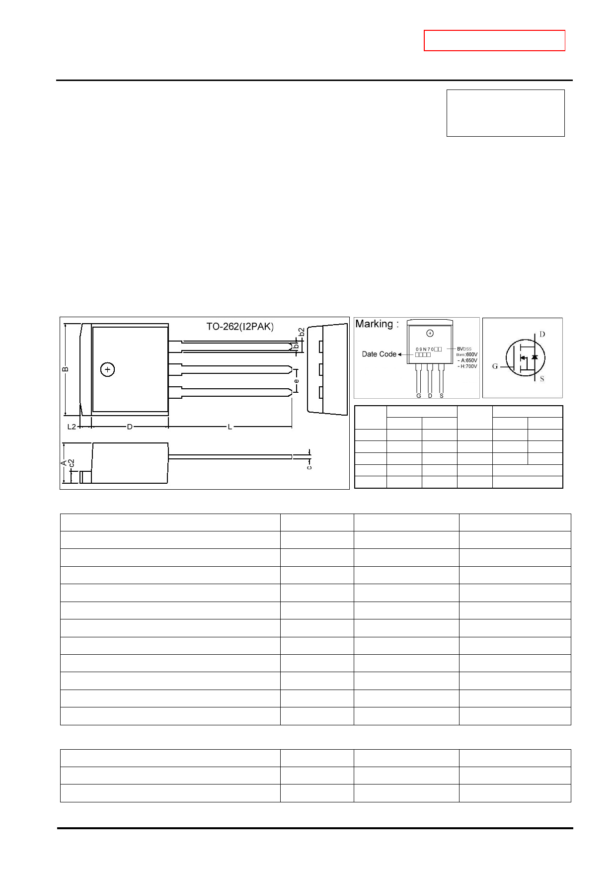
Package Dimensions
REF.
A
b
c
D
E
Millimeter
Min. Max.
4.40 4.80
0.76 1.00
0.36 0.50
8.60 9.00
9.80 10.4
REF.
c2
b2
L
e
L2
Millimeter
Min. Max.
1.25 1.45
1.17 1.47
13.25 14.25
2.54 REF.
1.27 REF.
Absolute Maximum Ratings
Parameter
Symbol
Drain-Source Voltage
- /A/H
VDS
Gate-Source Voltage
VGS
Continuous Drain Current , VGS@10V
ID @TC=25
Continuous Drain Current , VGS@10V
Pulsed Drain Current1
ID @TC=100
IDM
Total Power Dissipation
PD @TC=25
Linear Derating Factor
Single Pulse Avalanche Energy2
EAS
Avalanche Current
IAR
Repetitive Avalanche Energy
EAR
Operating Junction and Storage Temperature Range Tj, Tstg
Ratings
600/650/700
20
9
5
40
156
1.25
305
9
9
-55 ~ +150
Unit
V
V
A
A
A
W
W/
mJ
A
mJ
Thermal Data
Parameter
Thermal Resistance Junction-case
Thermal Resistance Junction-ambient
Max.
Max.
Symbol
Rthj-c
Rthj-a
Value
0.8
62
Unit
/W
/W
1/5
1 page 
ISSUED DATE :2005/04/21
REVISED DATE :
Fig 13. Switching Time Circuit
Fig 14. Switching Time Waveform
Fig 15. Gate Charge Circuit
Fig 16. Gate Charge Waveform
Important Notice:
All rights are reserved. Reproduction in whole or in part is prohibited without the prior written approval of GTM.
GTM reserves the right to make changes to its products without notice.
GTM semiconductor products are not warranted to be suitable for use in life-support Applications, or systems.
GTM assumes no liability for any consequence of customer product design, infringement of patents, or application assistance.
Head Office And Factory:
Taiwan: No. 17-1 Tatung Rd. Fu Kou Hsin-Chu Industrial Park, Hsin-Chu, Taiwan, R. O. C.
TEL : 886-3-597-7061 FAX : 886-3-597-9220, 597-0785
China: (201203) No.255, Jang-Jiang Tsai-Lueng RD. , Pu-Dung-Hsin District, Shang-Hai City, China
TEL : 86-21-5895-7671 ~ 4 FAX : 86-21-38950165
5/5
5 Page | ||
| Páginas | Total 5 Páginas | |
| PDF Descargar | [ Datasheet G2U09N70.PDF ] | |
Hoja de datos destacado
| Número de pieza | Descripción | Fabricantes |
| G2U09N70 | N-CHANNEL ENHANCEMENT MODE POWER MOSFET | GTM |
| Número de pieza | Descripción | Fabricantes |
| SLA6805M | High Voltage 3 phase Motor Driver IC. |
Sanken |
| SDC1742 | 12- and 14-Bit Hybrid Synchro / Resolver-to-Digital Converters. |
Analog Devices |
|
DataSheet.es es una pagina web que funciona como un repositorio de manuales o hoja de datos de muchos de los productos más populares, |
| DataSheet.es | 2020 | Privacy Policy | Contacto | Buscar |