|
|
|
PDF AD9920A Data sheet ( Hoja de datos )
| Número de pieza | AD9920A | |
| Descripción | 12-Bit CCD Signal Processor | |
| Fabricantes | Analog Devices | |
| Logotipo | ||
Hay una vista previa y un enlace de descarga de AD9920A (archivo pdf) en la parte inferior de esta página. Total 30 Páginas | ||
|
No Preview Available !
12-Bit CCD Signal Processor with V-Driver
and Precision Timing Generator
AD9920A
FEATURES
Integrated 19-channel V-driver
1.8 V AFETG core
24 programmable vertical clock signals
Correlated double sampler (CDS) with −3 dB, 0 dB,
+3 dB, and +6 dB gain
12-bit, 40.5 MHz analog-to-digital converter (ADC)
Black level clamp with variable level control
Complete on-chip timing generator
Precision Timing core with ~400 ps resolution
On-chip 3 V horizontal and RG drivers
General-purpose outputs (GPOs) for shutter and
system support
On-chip sync generator with external sync input
On-chip 1.8 V low dropout (LDO) regulator
105-ball, 8 mm × 8 mm CSP_BGA package
APPLICATIONS
Digital still cameras
GENERAL DESCRIPTION
The AD9920A is a highly integrated charge-coupled device (CCD)
signal processor for digital still camera applications. It includes a
complete analog front end (AFE) with analog-to-digital conversion,
combined with a full-function programmable timing generator
and 19-channel vertical driver (V-driver). The timing generator
is capable of supporting up to 24 vertical clock signals to control
advanced CCDs. The on-chip V-driver supports up to 19 channels
for use with six-field CCDs. A Precision Timing® core allows adjust-
ment of high speed clocks with approximately 400 ps resolution
at 40.5 MHz operation. The AD9920A also contains six GPOs
that can be used for shutter and system functions.
The analog front end includes black level clamping, variable
gain CDS, and a 12-bit ADC. The timing generator provides all
the necessary CCD clocks: RG, H-clocks, V-clocks, sensor gate
pulses, substrate clock, and substrate bias control.
The AD9920A is specified over an operating temperature range
of −25°C to +85°C.
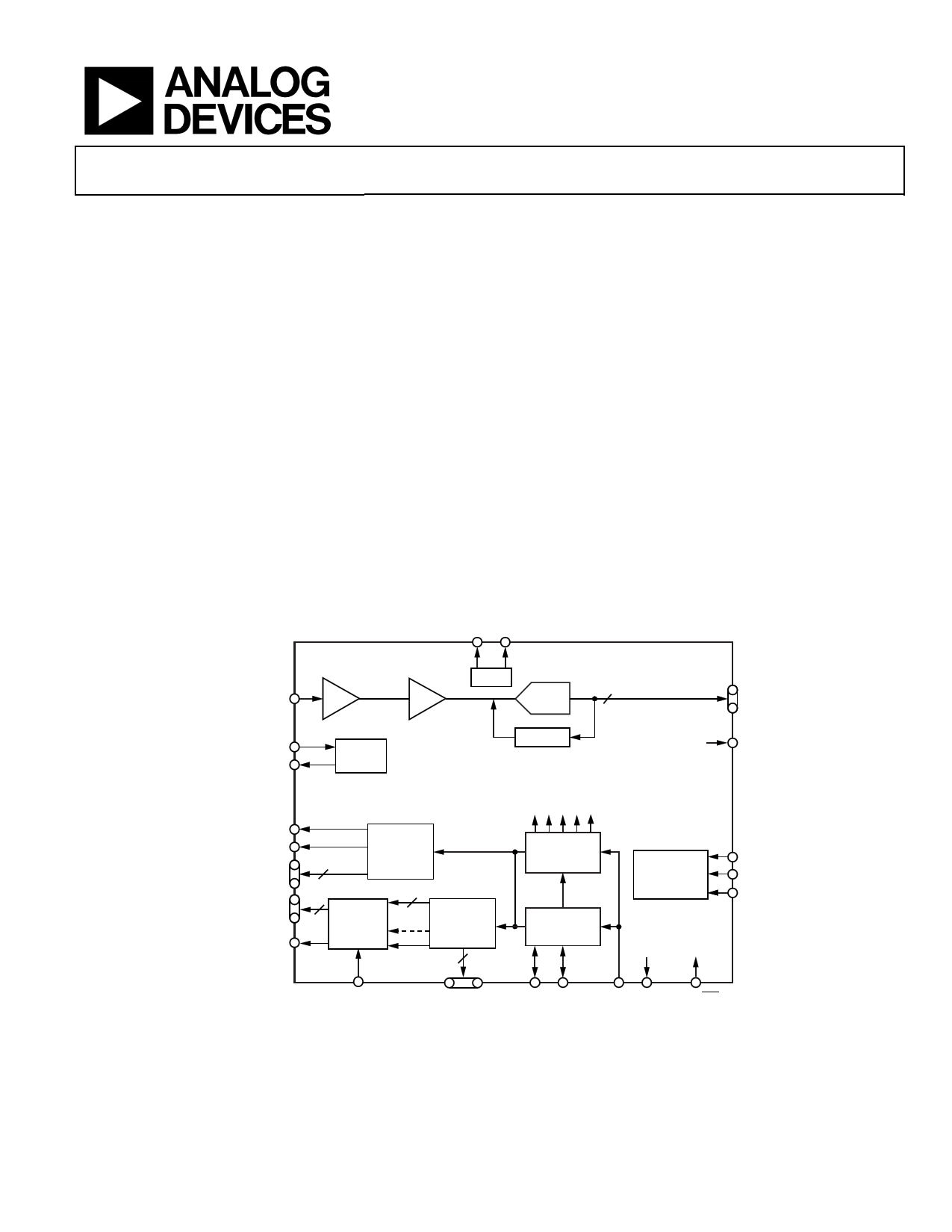
FUNCTIONAL BLOCK DIAGRAM
REFT REFB
–3dB, 0dB, +3dB, +6dB
CCDIN
CDS
VGA
LDOIN
LDOOUT
LDO
REG
6dB TO 42dB
VREF
12-BIT
ADC
CLAMP
12
AD9920A
D0 TO D11
DCLK
RG
HL
H1 TO H8
V1A TO V6 (3-LEVEL)
V7 TO V16 (2-LEVEL)
SUBCK
HORIZONTAL
8 DRIVERS
XV1 TO XV24
19
VERTICAL
DRIVER
24
GPO5
GPO6
VERTICAL
TIMING
CONTROL
XSUBCK 6
INTERNAL CLOCKS
PRECISION
TIMING
GENERATOR
SYNC
GENERATOR
INTERNAL
REGISTERS
SL
SCK
SDATA
XSUBCNT
GPO1 TO GPO4,
GPO7, GPO8
Figure 1.
HD VD
CLI CLO SYNC/RST
Rev. B
Information furnished by Analog Devices is believed to be accurate and reliable. However, no
responsibility is assumed by Analog Devices for its use, nor for any infringements of patents or other
rights of third parties that may result from its use. Specifications subject to change without notice. No
license is granted by implication or otherwise under any patent or patent rights of Analog Devices.
Trademarksandregisteredtrademarksarethepropertyoftheirrespectiveowners.
One Technology Way, P.O. Box 9106, Norwood, MA 02062-9106, U.S.A.
Tel: 781.329.4700
www.analog.com
Fax: 781.461.3113 ©2009–2010 Analog Devices, Inc. All rights reserved.
1 page 
AD9920A
SPECIFICATIONS
Table 1.
Parameter
TEMPERATURE RANGE
Operating
Storage
POWER SUPPLY VOLTAGE INPUTS
AVDD
TCVDD
CLIVDD
RGVDD
HVDD1 and HVDD2
DVDD
DRVDD
IOVDD
V-DRIVER POWER SUPPLY VOLTAGES
VDVDD
VH1, VH2
VL1, VL2
VM1, VM2
VLL
VH1, VH2 to VL1, VL2, VLL
VMM1
LDO2
LDOIN
Output Voltage
Output Current
POWER SUPPLY CURRENTS—40.5 MHz
OPERATION
AVDD
TCVDD
CLIVDD
RGVDD
HVDD1 and HVDD23
DVDD
DRVDD
IOVDD
POWER SUPPLY CURRENTS—STANDBY
MODE OPERATION
Standby1 Mode
Standby2 Mode
Standby3 Mode
MAXIMUM CLOCK RATE (CLI)
MINIMUM CLOCK RATE (CLI)
Test Conditions/Comments
AFE analog supply
Timing core supply
CLI input supply
RG, HL driver supply
H1 to H8 driver supplies
Digital logic supply
Parallel data output driver supply
Digital I/O supply
V-driver/logic supply
V-driver high supply
V-driver low supply
V-driver midsupply
SUBCK low supply
SUBCK midsupply
LDO supply input
1.8 V
1.8 V
3V
3.3 V, 20 pF RG load, 20 pF HL load
3.3 V, 480 pF total load on H1 to H8
1.8 V
3 V, 10 pF load on each data output pin
(D0 to D11)
3 V, depends on load and output
frequency of digital I/O
1 VMM must be greater than VLL and less than VDVDD.
2 LDO should be used only for the AD9920A 1.8 V supplies, not for external circuitry.
3 The total power dissipated by the HVDD (or RGVDD) can be approximated using the following equation:
Total HVDD Power = (CL × HVDD × Pixel Frequency) × HVDD
Min
−25
−65
1.6
1.6
1.6
2.1
2.1
1.6
1.6
1.6
1.6
11.0
−8.5
−1.5
−11.0
VLL
2.5
1.8
60
40.5
Typ
1.8
1.8
3.0
3.0
3.0
1.8
3.0
3.0
3.0
15.0
−7.5
0.0
−7.5
0.0
3.0
1.9
100
27
5
1.5
10
59
9.5
6
2
20
5
1.5
10
Max
+85
+150
2.0
2.0
3.6
3.6
3.6
2.0
3.6
3.6
3.6
16.5
−5.5
+1.5
−5.5
23.5
VDVDD
3.6
2.05
Unit
°C
°C
V
V
V
V
V
V
V
V
V
V
V
V
V
V
V
V
V
mA
mA
mA
mA
mA
mA
mA
mA
mA
mA
mA
mA
MHz
MHz
Rev. B | Page 4 of 112
5 Page 
AD9920A
ABSOLUTE MAXIMUM RATINGS
Table 6.
Parameter
AVDD to AVSS
TCVDD to TCVSS
HVDD1, HVDD2 to HVSS1, HVSS2
RGVDD to RGVSS
DVDD to DVSS
DRVDD to DRVSS/LDOVSS
IOVDD to IOVSS
VDVDD to VDVSS
CLIVDD to TCVSS
VH1, VH2 to VL1, VL2, VLL
VH1, VH2 to VDVSS
VL1, VL2 to VDVSS
VM1, VM2 to VDVSS
VLL to VDVSS
VMM to VDVSS
V1A to V16 to VDVSS
RG and HL Outputs to RGVSS
H1 to H8 Outputs to HVSSx
VDR_EN, XSUBCNT, SRCTL, SRSW
to VDVSS
Digital Outputs to IOVSS
Digital Inputs to IOVSS
SCK, SL, SDATA to DVSS
REFT, REFB, CCDIN to AVSS
Junction Temperature
Lead Temperature
(Soldering, 10 sec)
Rating
−0.3 V to +2.2 V
−0.3 V to +2.2 V
−0.3 V to +3.9 V
−0.3 V to +3.9 V
−0.3 V to +2.2 V
−0.3 V to +3.9 V
−0.3 V to +3.9 V
−0.3 V to +3.9 V
−0.3 V to +3.9 V
−0.3 V to +25.0 V
−0.3 V to +17.0 V
−17.0 V to +0.3 V
−6.0 V to +3.0 V
−17.0 V to +0.3 V
VLL − 0.3 V to VDVDD + 0.3 V
VLx − 0.3 V to VHx + 0.3 V
−0.3 V to RGVDD + 0.3 V
−0.3 V to HVDDx + 0.3 V
−0.3 V to VDVDD + 0.3 V
−0.3 V to IOVDD + 0.3 V
−0.3 V to IOVDD + 0.3 V
−0.3 V to DVDD + 0.3 V
−0.3 V to AVDD + 0.3 V
150°C
350°C
Stresses above those listed under Absolute Maximum Ratings
may cause permanent damage to the device. This is a stress
rating only; functional operation of the device at these or any
other conditions above those indicated in the operational
section of this specification is not implied. Exposure to absolute
maximum rating conditions for extended periods may affect
device reliability.
THERMAL RESISTANCE
θJA is specified for the worst-case conditions, that is, a device
soldered in a circuit board for surface-mount packages.
Table 7. Thermal Resistance
Package Type
θJA Unit
CSP_BGA (BC-105-1)
40.3 °C/W
ESD CAUTION
Rev. B | Page 10 of 112
11 Page | ||
| Páginas | Total 30 Páginas | |
| PDF Descargar | [ Datasheet AD9920A.PDF ] | |
Hoja de datos destacado
| Número de pieza | Descripción | Fabricantes |
| AD9920A | 12-Bit CCD Signal Processor | Analog Devices |
| Número de pieza | Descripción | Fabricantes |
| SLA6805M | High Voltage 3 phase Motor Driver IC. |
Sanken |
| SDC1742 | 12- and 14-Bit Hybrid Synchro / Resolver-to-Digital Converters. |
Analog Devices |
|
DataSheet.es es una pagina web que funciona como un repositorio de manuales o hoja de datos de muchos de los productos más populares, |
| DataSheet.es | 2020 | Privacy Policy | Contacto | Buscar |