|
|
|
PDF ICSSSTUA32S869B Data sheet ( Hoja de datos )
| Número de pieza | ICSSSTUA32S869B | |
| Descripción | 14-Bit Configurable Registered Buffer | |
| Fabricantes | ICS | |
| Logotipo | ||
Hay una vista previa y un enlace de descarga de ICSSSTUA32S869B (archivo pdf) en la parte inferior de esta página. Total 18 Páginas | ||
|
No Preview Available !
www.DataSheet4U.com
Integrated
Circuit
Systems, Inc.
ICSSSTUA32S869B
Advance Information
14-Bit Configurable Registered Buffer for DDR2
Recommended Application:
• DDR2 Memory Modules
• Provides complete DDR DIMM solution with
ICS97U877
• Ideal for DDR2 400, 533 and 667
Product Features:
• 14-bit 1:2 registered buffer with parity check
functionality
• Supports SSTL_18 JEDEC specification on data
inputs and outputs
• 50% more dynamic driver strength than standard
SSTU32864
• Supports LVCMOS switching levels on C1 and
RESET# inputs
• Low voltage operation
VDD = 1.7V to 1.9V
• Available in 150 BGA package
• Green packages available
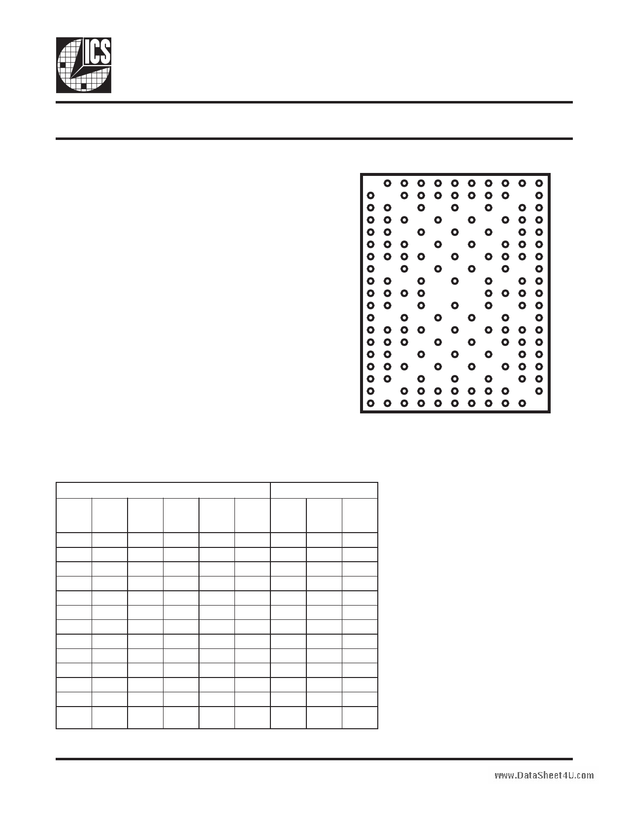
Pin Configuration
1 2 3 4 5 6 7 8 9 10 11
A
B
C
D
E
F
G
H
J
K
L
M
N
P
R
T
U
V
W
150 Ball BGA
(Top View)
Functionality Truth Table
Inputs
Outputs
RESET# DCS# CSR# CK
CK#
Dn,
DODT,
DCKE
Qn
QCS#
QODT,
QCKE
HL L ↑↓L L L L
HL L ↑↓HHLH
H
L
L L or H L or H X
Q0 Q0 Q0
HLH↑↓L L L L
H L H ↑↓HH L H
H
L
H L or H L or H X
Q0 Q0 Q0
HHL↑↓L LHL
HHL ↑↓HHHH
H
H
L L or H L or H X
Q0 Q0 Q0
H H H ↑ ↓ L Q0 H L
H H H ↑ ↓ H Q0 H H
H H H L or H L or H X Q0 Q0 Q0
L
X or X or X or X or X or
floating floating floating floating floating
L
L
L
1173—10/28/05
ADVANCE INFORMATION documents contain information on products in the formative or design phase development. Characteristic data and other specifications are design goals.
ICS reserves the right to change or discontinue these products without notice. Third party brands and names are the property of their respective owners.
1 page 
ICSSSTUA32S869B
Advance Information
Terminal Functions
Signal Group Signal Name
Ungated inputs DCKE, DODT
Chip Select
gated inputs
D1 ... D14(1)
Chip Select
inputs
DCS#, CSR#
Type
SSTL_18
SSTL_18
SSTL_18
Re-driven
outputs
Parity input
Q1A...Q14A,
SSTL_18
Q1B ... Q14B,
QCSA#, QCSB#
QCKEA,QCKEB
QODTA,QODTB
PARIN1
SSTL_18
Parity output PPO1
SSTL_18
Description
DRAM function pins not associated with Chip Select.
DRAM inputs, re-driven only when Chip Select is LOW.
DRAM Chip Select signals. This pins initiate DRAM address/
command decodes, and as such at least one will be low when
a valid address/command is present.
Outputs of the register, valid after the specified clock count
and immediately following a rising edge of the clock.
Inout parity is received on pin PARIN1 and should maintain
parity across the D1...D14(1) inputs, at the rising edge of the
clock, one cycle after Chip Select is LOW.
Partial Parity Output. Indicates parity out of D1-D14(1)
Parity error
output
PTYERR1#
Open drain
When LOW, this output indicates that a parity error was
identified associated with the address and/or command inputs.
PTYERR1# will be active for two clock cycles, and delayed
by in total 2 clock cycles for compatibility with final parity
out timing on the industry-standard DDR2 register with
parity (in JEDEC definition).
Configuration C1
Inputs
1.8V
LVCMOS
When Low, register is configured as Register 1. When High,
register is confugured as Register 2.
Clock inputs CK, CK#
SSTL_18
Differential master clock input pair to the register. The
register operation is triggered by a rising edge on the positive
clock input (CK).
Miscellaneous RESET#
inputs
1.8 V
LVCMOS
Asynchronous reset input. When LOW, it causes a reset of the
internal latches, thereby forcing the outputs LOW. RESET#
also resets the PTYERR# signal.
VREF
0.9 V nominal Input reference voltage for the SSTL_18 inputs. Two pins
(internally tied together) are used for increased reliability.
VDD
Power Input Power supply voltage
GND
Ground Input Ground
NOTE 1 Inputs D1, D4 and D7 and their corresponding outputs Qn are not included in this range.
1173—10/28/05
5
5 Page 
ICSSSTUA32S869B
Advance Information
Electrical Characteristics - DC
TA = 0 - 70°C; VDD = 2.5 +/-0.2V, VDDQ=2.5 +/-0.2V; (unless otherwise stated)
SYMBOL PARAMETERS
CONDITIONS
VDDQ
VIK II = -18mA
VOH
IOH = -100µA
IOH = 6mA
1.7V
1.7V
VOL
IOL = 100µA
IOL = 6mA
1.7V
1.7V
II All Inputs
VI = VDD or GND
1.9V
Standby (Static)
RESET# = GND
IDD Operating (Static) VI = VIH(AC) or VIL(AC),
RESET# = VDD
1.9V
RESET# = VDD,
Dynamic operating VI = VIH(AC) or VIL(AC),
(clock only)
CLK and CLK# switching
50% duty cycle.
RESET# = VDD,
IO = 0
IDDD
VI = VIH(AC) or VIL (AC),
Dynamic Operating CLK and CLK# switching
(per each data input) 50% duty cycle. One data
input switching at half
1.8V
clock frequency, 50%
duty cycle
Input capacitance,
Dn, PAR_IN inputs VI = VREF ± 250 mV
Input capacitance,
DCS#n
VI = VREF ± 250 mV
Input capacitance,
Ci CK and CK# inputs2 VICR = 0.9V; VI(PP) = 600 mV
1.8V
Input capacitance,
RESET# input
VI = VDD or GND
Data Inputs
CLK and CLK#
RESET#
VI = VREF ±350mV
VICR = 1.25V, VI(PP) = 360mV
VI = VDDQ or GND
Notes:
1 - Guaranteed by design, not 100% tested in production.
2 - The vendor must supply this value for full device description.
MIN TYP
VDDQ - 0.2
1.2
MAX
-1.2
0.2
0.5
±5
0.2
TBD
UNITS
V
µA
µA
mA
TBD
µ/clock
MHz
TBD
µA/ clock
MHz/data
2.5
2
2
Note 2
2.5
2
3.5
3
3
Note 2
3.5
3
2.5
pF
pF
pF
pF
pF
Output Buffer Characteristics
Output edge rates over recommended operating free-air temperature range (See figure 7)
PARAMETER
VDD = 1.8V ± 0.1V
MIN MAX
UNIT
dV/dt_r
1
4
V/ns
dV/dt_f
dV/dt_∆1
1
4
1
V/ns
V/ns
1. Difference between dV/dt_r (rising edge rate) and dV/dt_f (falling edge rate)
1173—10/28/05
11
11 Page | ||
| Páginas | Total 18 Páginas | |
| PDF Descargar | [ Datasheet ICSSSTUA32S869B.PDF ] | |
Hoja de datos destacado
| Número de pieza | Descripción | Fabricantes |
| ICSSSTUA32S869B | 14-Bit Configurable Registered Buffer | ICS |
| Número de pieza | Descripción | Fabricantes |
| SLA6805M | High Voltage 3 phase Motor Driver IC. |
Sanken |
| SDC1742 | 12- and 14-Bit Hybrid Synchro / Resolver-to-Digital Converters. |
Analog Devices |
|
DataSheet.es es una pagina web que funciona como un repositorio de manuales o hoja de datos de muchos de los productos más populares, |
| DataSheet.es | 2020 | Privacy Policy | Contacto | Buscar |