|
|
|
PDF MC1455B Data sheet ( Hoja de datos )
| Número de pieza | MC1455B | |
| Descripción | Timers | |
| Fabricantes | ON Semiconductor | |
| Logotipo | ||
Hay una vista previa y un enlace de descarga de MC1455B (archivo pdf) en la parte inferior de esta página. Total 11 Páginas | ||
|
No Preview Available !
MC1455, MC1455B,
NCV1455B
Timers
The MC1455 monolithic timing circuit is a highly stable controller
capable of producing accurate time delays or oscillation. Additional
terminals are provided for triggering or resetting if desired. In the time
delay mode, time is precisely controlled by one external resistor and
capacitor. For astable operation as an oscillator, the free−running
frequency and the duty cycle are both accurately controlled with two
external resistors and one capacitor. The circuit may be triggered and
reset on falling waveforms, and the output structure can source or sink
up to 200 mA or drive TTL circuits.
Features
• Direct Replacement for NE555 Timers
• Timing from Microseconds through Hours
• Operates in Both Astable and Monostable Modes
• Adjustable Duty Cycle
• High Current Output Can Source or Sink 200 mA
• Output Can Drive TTL
• Temperature Stability of 0.005% per °C
• Normally ON or Normally OFF Output
• Pb−Free Packages are Available
10 k
0.1 mF
5
0.01 mF
1.0 k
38
4 6R
2 MC1455 7
1 1.0 mF
MT2
20 M G
C
-10 V
Load
MT1
1N4003
http://onsemi.com
MARKING
DIAGRAMS
8
1
SOIC−8
D SUFFIX
CASE 751
8
1455x
ALYW
G
1
8
1
PDIP−8
P1 SUFFIX
CASE 626
8
MC1455yyy
AWL
YYWWG
1
x = B or V
yyy = BP1 or P1
A = Assembly Location
L = Wafer Lot
Y, YY = Year
W, WW = Work Week
G or G = Pb−Free Package
ORDERING INFORMATION
See detailed ordering and shipping information in the package
dimensions section on page 9 of this data sheet.
t = 1.1; R and C = 22 sec
Time delay (t) is variable by
changing R and C (see Figure 16).
1N4740
3.5 k
-
10
mF
250 V +
VR ICC VCC
Figure 1. 22 Second Solid State Time Delay Relay Circuit
VCC
8
5k
6
Threshold
5
Control Voltage
5k
Trigger
2
5k
+
Comp
-A
+
Comp
-B
1
GND
Flip
R Flop
Q
S Inhibit/
Reset
4
Reset
7
Discharge
3
Output
+
0.01 mF
VO
Reset
5
Control
Voltage
3
Output
ISink
ISource
48
VCC 7
700
Discharge
MC1455
Threshold
6 Ith
GND Trigger
12
2.0 k
VS
Test circuit for measuring DC parameters (to set output and measure
parameters):
a) When VS w 2/3 VCC, VO is low.
b) When VS v 1/3 VCC, VO is high.
c) When VO is low, Pin 7 sinks current. To test for Reset, set VO
c) high, apply Reset voltage, and test for current flowing into Pin 7.
c) When Reset is not in use, it should be tied to VCC.
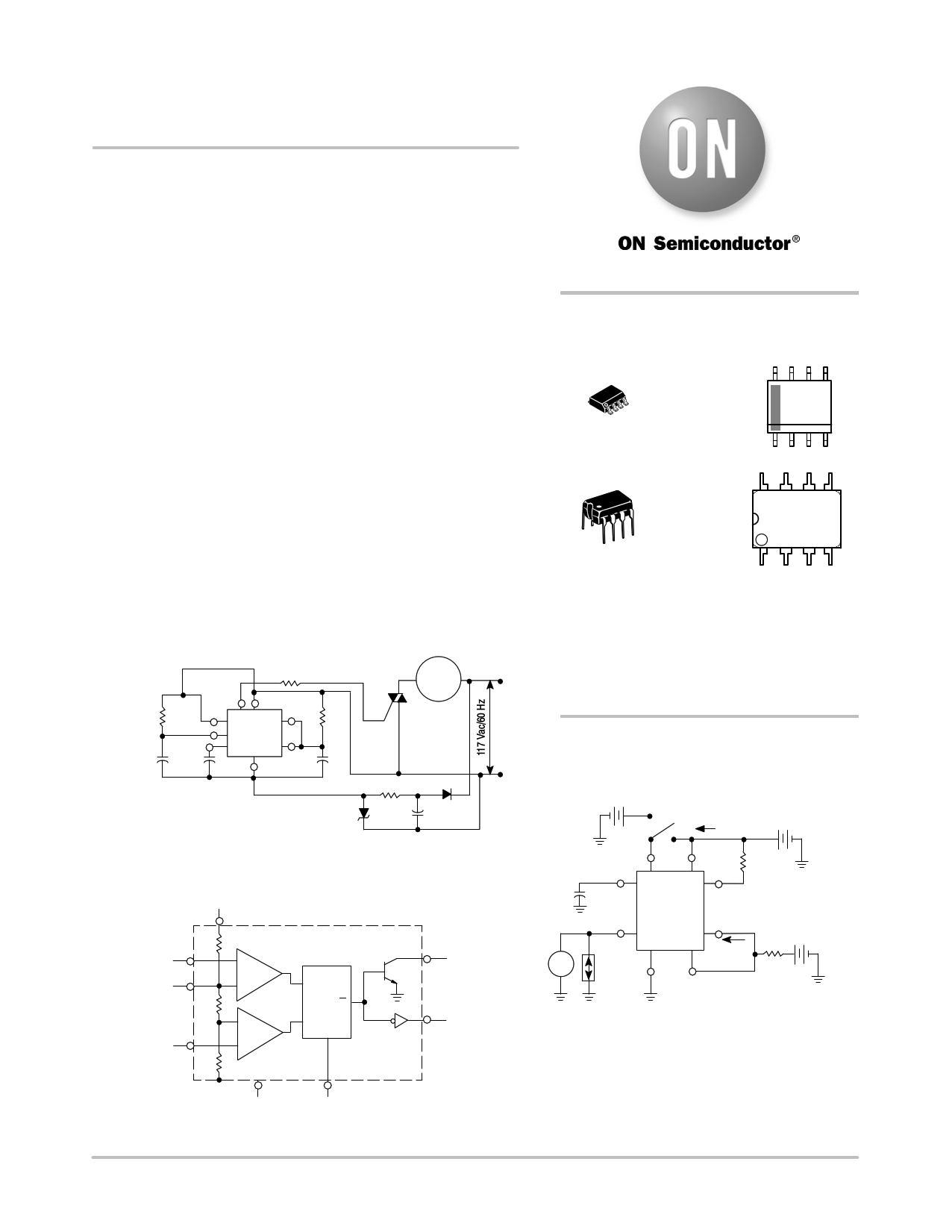
Figure 2. Representative Block Diagram
Figure 3. General Test Circuit
© Semiconductor Components Industries, LLC, 2009
December, 2009 − Rev. 10
1
Publication Order Number:
MC1455/D
1 page 
MC1455, MC1455B, NCV1455B
Control Voltage
Threshold
Comparator
Trigger
Comparator
Flip-Flop
Output
VCC
4.7 k 830 4.7 k 1.0 k
6.8 k
5.0 k
Threshold
7.0 k
Trigger
Reset
Discharge
GND
10 k
cb
5.0 k e 4.7 k
Reset
Discharge
100 k
100
5.0 k
Figure 13. Representative Circuit Schematic
3.9 k
cb
Output
220
4.7 k
GENERAL OPERATION
The MC1455 is a monolithic timing circuit which uses an
external resistor − capacitor network as its timing element. It
can be used in both the monostable (one−shot) and astable
modes with frequency and duty cycle controlled by the
capacitor and resistor values. While the timing is dependent
upon the external passive components, the monolithic circuit
provides the starting circuit, voltage comparison and other
functions needed for a complete timing circuit. Internal to the
integrated circuit are two comparators, one for the input
signal and the other for capacitor voltage; also a flip−flop and
digital output are included. The comparator reference
voltages are always a fixed ratio of the supply voltage thus
providing output timing independent of supply voltage.
Monostable Mode
In the monostable mode, a capacitor and a single resistor
are used for the timing network. Both the threshold terminal
and the discharge transistor terminal are connected together
in this mode (refer to circuit in Figure 14). When the input
voltage to the trigger comparator falls below 1/3 VCC, the
comparator output triggers the flip−flop so that its output sets
low. This turns the capacitor discharge transistor “off” and
drives the digital output to the high state. This condition
allows the capacitor to charge at an exponential rate which is
set by the RC time constant. When the capacitor voltage
reaches 2/3 VCC, the threshold comparator resets the
flip−flop. This action discharges the timing capacitor and
returns the digital output to the low state. Once the flip−flop
has been triggered by an input signal, it cannot be retriggered
until the present timing period has been completed. The time
that the output is high is given by the equation t = 1.1 RA C.
Various combinations of R and C and their associated times
are shown in Figure 16. The trigger pulse width must be less
than the timing period.
A reset pin is provided to discharge the capacitor, thus
interrupting the timing cycle. As long as the reset pin is low,
the capacitor discharge transistor is turned “on” and prevents
the capacitor from charging. While the reset voltage is applied
the digital output will remain the same. The reset pin should
be tied to the supply voltage when not in use.
+VCC (5.0 V to 15 V)
Reset
RL 4
Output
VCC
8
Discharge
7
RA
3
RL 2
Trigger
MC1455
1
6
Threshold
5
Control
Voltage
C
0.01 mF
Figure 14. Monostable Circuit
http://onsemi.com
5
5 Page 
MC1455, MC1455B, NCV1455B
PACKAGE DIMENSIONS
PDIP−8
P1 SUFFIX
CASE 626−05
ISSUE L
NOTE 2
85
14
F
−A−
−B−
−T−
SEATING
PLANE
H
C
N
D
G
K
0.13 (0.005) M T A M B M
L
J
M
NOTES:
1. DIMENSION L TO CENTER OF LEAD WHEN
FORMED PARALLEL.
2. PACKAGE CONTOUR OPTIONAL (ROUND OR
SQUARE CORNERS).
3. DIMENSIONING AND TOLERANCING PER ANSI
Y14.5M, 1982.
MILLIMETERS
INCHES
DIM MIN MAX MIN MAX
A 9.40 10.16 0.370 0.400
B 6.10 6.60 0.240 0.260
C 3.94 4.45 0.155 0.175
D 0.38 0.51 0.015 0.020
F 1.02 1.78 0.040 0.070
G 2.54 BSC
0.100 BSC
H 0.76 1.27 0.030 0.050
J 0.20 0.30 0.008 0.012
K 2.92 3.43 0.115 0.135
L 7.62 BSC
0.300 BSC
M --- 10_ --- 10_
N 0.76 1.01 0.030 0.040
ON Semiconductor and
are registered trademarks of Semiconductor Components Industries, LLC (SCILLC). SCILLC reserves the right to make changes without further notice
to any products herein. SCILLC makes no warranty, representation or guarantee regarding the suitability of its products for any particular purpose, nor does SCILLC assume any liability
arising out of the application or use of any product or circuit, and specifically disclaims any and all liability, including without limitation special, consequential or incidental damages.
“Typical” parameters which may be provided in SCILLC data sheets and/or specifications can and do vary in different applications and actual performance may vary over time. All
operating parameters, including “Typicals” must be validated for each customer application by customer’s technical experts. SCILLC does not convey any license under its patent rights
nor the rights of others. SCILLC products are not designed, intended, or authorized for use as components in systems intended for surgical implant into the body, or other applications
intended to support or sustain life, or for any other application in which the failure of the SCILLC product could create a situation where personal injury or death may occur. Should
Buyer purchase or use SCILLC products for any such unintended or unauthorized application, Buyer shall indemnify and hold SCILLC and its officers, employees, subsidiaries, affiliates,
and distributors harmless against all claims, costs, damages, and expenses, and reasonable attorney fees arising out of, directly or indirectly, any claim of personal injury or death
associated with such unintended or unauthorized use, even if such claim alleges that SCILLC was negligent regarding the design or manufacture of the part. SCILLC is an Equal
Opportunity/Affirmative Action Employer. This literature is subject to all applicable copyright laws and is not for resale in any manner.
PUBLICATION ORDERING INFORMATION
LITERATURE FULFILLMENT:
Literature Distribution Center for ON Semiconductor
P.O. Box 5163, Denver, Colorado 80217 USA
Phone: 303−675−2175 or 800−344−3860 Toll Free USA/Canada
Fax: 303−675−2176 or 800−344−3867 Toll Free USA/Canada
Email: [email protected]
N. American Technical Support: 800−282−9855 Toll Free
USA/Canada
Europe, Middle East and Africa Technical Support:
Phone: 421 33 790 2910
Japan Customer Focus Center
Phone: 81−3−5773−3850
http://onsemi.com
11
ON Semiconductor Website: www.onsemi.com
Order Literature: http://www.onsemi.com/orderlit
For additional information, please contact your local
Sales Representative
MC1455/D
11 Page | ||
| Páginas | Total 11 Páginas | |
| PDF Descargar | [ Datasheet MC1455B.PDF ] | |
Hoja de datos destacado
| Número de pieza | Descripción | Fabricantes |
| MC1455 | Timers | ON Semiconductor |
| MC1455 | Timing Circuit | Motorola Semiconductors |
| MC1455 | Timers | ON Semiconductor |
| MC1455 | Timing Circuits | Motorola Semiconductors |
| Número de pieza | Descripción | Fabricantes |
| SLA6805M | High Voltage 3 phase Motor Driver IC. |
Sanken |
| SDC1742 | 12- and 14-Bit Hybrid Synchro / Resolver-to-Digital Converters. |
Analog Devices |
|
DataSheet.es es una pagina web que funciona como un repositorio de manuales o hoja de datos de muchos de los productos más populares, |
| DataSheet.es | 2020 | Privacy Policy | Contacto | Buscar |