|
|
|
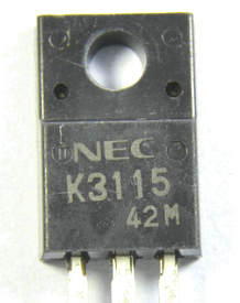
PDF K3115 Data sheet ( Hoja de datos )
| Número de pieza | K3115 | |
| Descripción | MOSFET ( Transistor ) - 2SK3115 | |
| Fabricantes | NEC | |
| Logotipo | ||
 1. Power MOSFET, 2SK3115 - NEC Hay una vista previa y un enlace de descarga de K3115 (archivo pdf) en la parte inferior de esta página. Total 8 Páginas | ||
|
No Preview Available !
www.DataSheet4U.com
DATA SHEET
MOS FIELD EFFECT TRANSISTOR
2SK3115
SWITCHING
N-CHANNEL POWER MOS FET
INDUSTRIAL USE
DESCRIPTION
The 2SK3115 is N-Channel DMOS FET device that features a low gate charge and excellent switching haracteristics, and
designed for high voltage applications such as switching power supply, AC adapter.
FEATURES
• Low gate charge
QG = 26 nC TYP. (VDD = 450 V, VGS = 10 V, ID = 6.0 A)
• Gate voltage rating ±30 V
• Low on-state resistance
RDS(on) = 1.2 Ω MAX. (VGS = 10 V, ID = 3.0 A)
• Avalanche capability ratings
ORDERING INFORMATION
PART NUMBER
PACKAGE
2SK3115
Isolated TO-220
5 (Isolated TO-220)
ABSOLUTE MAXIMUM RATINGS (TA = 25°C)
Drain to Source Voltage (VGS = 0 V)
VDSS
Gate to Source Voltage (VDS = 0 V)
VGSS
Drain Current (DC) (TC = 25°C)
Drain Current (pulse) Note1
ID(DC)
ID(pulse)
Total Power Dissipation (TA = 25°C)
PT1
Total Power Dissipation (TC = 25°C)
PT2
Channel Temperature
Tch
Storage Temperature
Single Avalanche Current Note2
Single Avalanche Energy Note2
Tstg
IAS
EAS
600
±30
±6.0
±24
2.0
35
150
−55 to +150
6.0
24
V
V
A
A
W
W
°C
°C
A
mJ
Notes 1. PW ≤ 10 µs, Duty Cycle ≤ 1%
2. Starting Tch = 25°C, VDD = 150 V, RG = 25 Ω, VGS = 20 → 0 V
The information in this document is subject to change without notice. Before using this document, please
confirm that this is the latest version.
Not all devices/types available in every country. Please check with local NEC representative for
availability and additional information.
Document No. D13338EJ2V0DS00 (2nd edition)
Date Published January 2001 NS CP (K)
Printed in Japan
The mark 5 shows major revised points.
©
1998, 2001
1 page 
www.DataSheet4U.com
2SK3115
DRAIN TO SOURCE ON-STATE RESISTANCE vs.
CHANNEL TEMPERATURE
3.0
ID = 6.0 A
3.0 A
2.0
1.0
0
−50
VGS = 10 V
Pulsed
0 50 100 150
Tch - Channel Temperature - ˚C
CAPACITANCE vs. DRAIN TO
SOURCE VOLTAGE
10000
1000
Ciss
100 Coss
10
VGS = 0 V
f = 1 MHz
1
1.0
10
100
Crss
VDS - Drain to Source Voltage - V
1000
10000
REVERSE RECOVERY TIME vs.
DRAIN CURRENT
di/dt = 50 A/µs
VGS = 0 V
1000
100
10
0.1 1.0 10 100
ID - Drain Current - A
SOURCE TO DRAIN DIODE FORWARD VOLTAGE
100
10
1.0
VGS = 10 V 0 V
0.1
Pulsed
0 0.5 1.0 1.5
VSD - Source to Drain Voltage - V
SWITCHING CHARACTERISTICS
100
td(off)
tf
10 td(on)
1
0.1
0.1
tr
VDD = 150 V
VGS = 10 V
RG = 10 Ω
1 10
ID - Drain Current - A
DYNAMIC INPUT/OUTPUT CHARACTERISTICS
16
ID = 6 A
14
600 VDD = 450 V
300 V
120 V
VGS
12
10
400 8
6
200
VDS
4
2
0
0 10 20 30 40
Qg - Gate Charge - nC
Data Sheet D13338EJ2V0DS
5
5 Page | ||

| Páginas | Total 8 Páginas | |
| PDF Descargar | [ Datasheet K3115.PDF ] | |
Hoja de datos destacado
| Número de pieza | Descripción | Fabricantes |
| K3113 | MOSFET ( Transistor ) - 2SK3113 | NEC |
| K3114 | MOSFET ( Transistor ) - 2SK3114 | NEC |
| K3115 | MOSFET ( Transistor ) - 2SK3115 | NEC |
| K3115B | N-CHANNEL POWER MOS FET | Renesas |
| Número de pieza | Descripción | Fabricantes |
| SLA6805M | High Voltage 3 phase Motor Driver IC. |
Sanken |
| SDC1742 | 12- and 14-Bit Hybrid Synchro / Resolver-to-Digital Converters. |
Analog Devices |
|
DataSheet.es es una pagina web que funciona como un repositorio de manuales o hoja de datos de muchos de los productos más populares, |
| DataSheet.es | 2020 | Privacy Policy | Contacto | Buscar |