|
|
|
PDF CH7024 Data sheet ( Hoja de datos )
| Número de pieza | CH7024 | |
| Descripción | (CH7023 / CH7024) TV Encoder | |
| Fabricantes | Chrontel | |
| Logotipo | ||
Hay una vista previa y un enlace de descarga de CH7024 (archivo pdf) en la parte inferior de esta página. Total 10 Páginas | ||
|
No Preview Available !
www.DataSheet4U.com
Chrontel
CH7023/CH7024
Brief Datasheet
CH7023/CH7024 TV Encoder
Features
• TV encoder targeting handheld and similar systems
• Support for NTSC, PAL
• Video output support for CVBS or S-video
• Macrovision™ 7.1.L1 copy protection support for
SDTV (CH7023 only)
• Programmable 24-bit/18-bit/16-bit/15-bit/12-bit/8-bit
digital input interface supporting various RGB and
YCrCb (e.g. RGB565, RGB666, RGB888, ITU656
like YCrCb, etc.) input data formats
• Support for input resolutions up to 720x480 and
720x576 (e.g. 220x176, 320x240, 640x480, 720x480,
720x576, etc.)
• Adjustable brightness, contrast, hue and saturation.
• Detect TV / Monitor connection
• Two high quality10-bit video DAC outputs
• Fully programmable through serial port
• Flexible pixel clock frequency from graphics
controller (2.3MHz—64MHz)
• Flexible input clock on the crystal or oscillator
(2.3MHz—64MHz)
• Flexible up and down scaling on the display
• Master and slave mode
• Offered in 48-pin LQFP and 49-pin TFBGA Package
• IO voltage and SPC/SPD from 1.2V to 3.3V
• Programmable power management
• Power down current less than 20uA typical
• Power consumption of <150mW for one CVBS
output, single terminated and <350mW for two DAC
outputs, double terminated.
General Description
The CH7023/CH7024 is a TV encoder device targeting
handheld, portable video applications such as digital
still cameras and similar portable embedded systems.
The device is able to encode the video signals and
generate synchronization signals for NTSC and PAL
standards.
Supported TV output formats are NTSC-M, NTSC-J,
NTSC-433, PAL-B/D/G/A/I, PAL-M, PAL-N and PAL-
60.
The device accepts different data formats including
RGB and YCrCb (e.g. RGB565, RGB666, RGB888,
ITU656 like YCrCb, etc.) via 24 bit/18 bit/15 bit /12 bit
/8 bit multiplexed digital inputs. Most embedded
controllers are supported. The I/O interface voltage
between CH7023/CH7024 and digital video source
controller can be selected by the I/O supply voltage
(VDDIO). The I/O supply voltage range is from 1.2V to
3.3V. The digital input voltage will follow the I/O
supply voltage.
CH7023/CH7024 is offered in both 48-pin LQFP
package (7 x 7 mm) and 49-pin TFBGA package (6 x 6
mm). CH7023/CH7024 48-pin LQFP package comes
with fixed single serial port address while 49-pin
TFBGA package provide two user selectable serial port
addresses via AS pin pull up or pull down option. Refer
to application note AN-98 for more information.
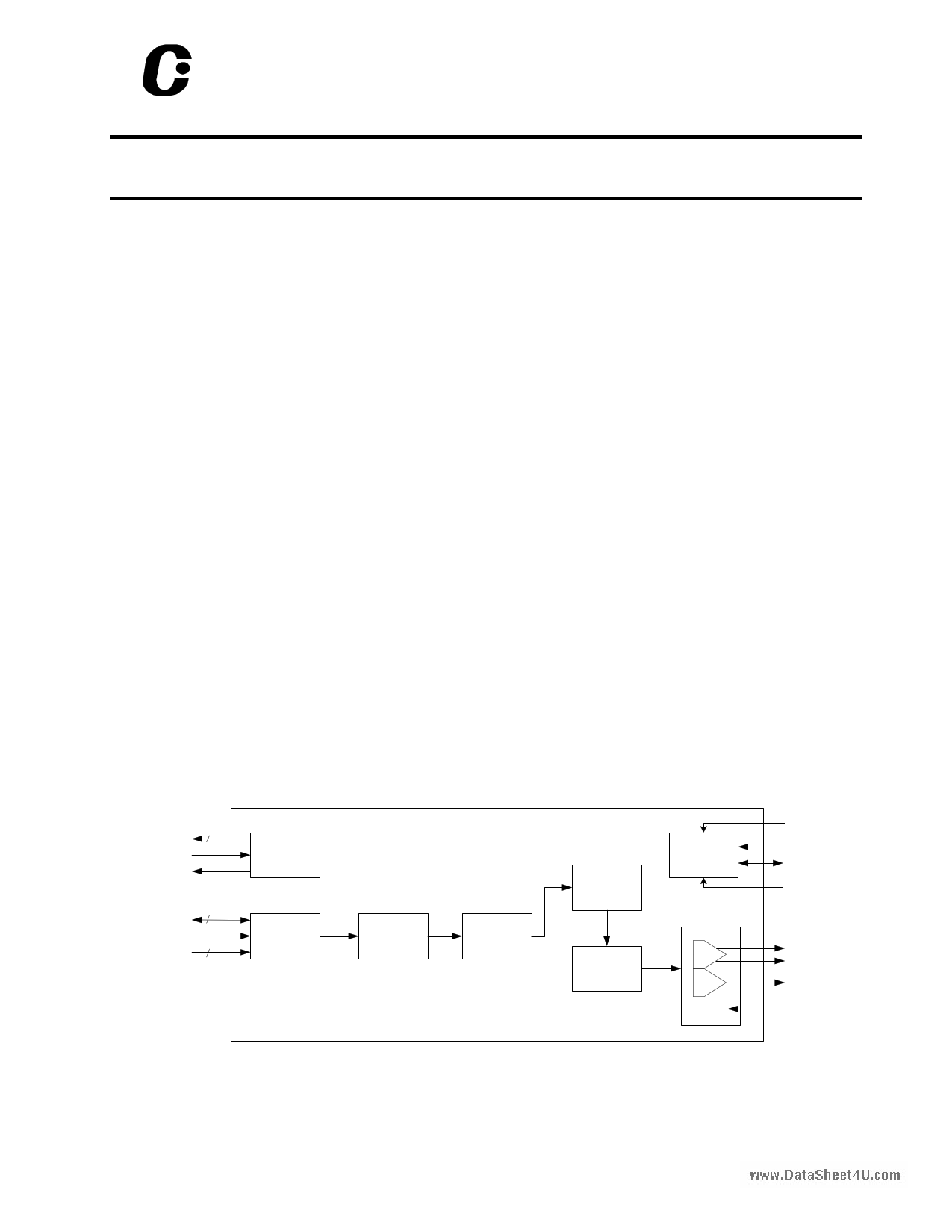
XIN/FIN,XO
XCLK
P-OUT
2
PLL
H,V
DE
D[23:0]
2
24
Data Demux
CSC
Line Memory
Based Scaler
Sync
Generation
TV Signal
Formatter
Serial Port
Control
DAC 0
DAC 1
Two
10-bit DAC’s
RESET*
SPC
SPD
AS
CVBS
Y
C
ISET
Figure 1: CH7023/CH7024 Block Diagram
209-0000-062 Rev. 1.14, 6/8/2007
1
1 page 
www.DataSheet4U.com
CHRONTEL
CH7023/CH7024
Table 1: Pin Description (cont’d)
Pin #
26
30
37
34
35
41
38
16
18
25
29
32
31
33
36
Type
Out
In
Out
In
Out
In
Power
Power
Power
Power
Power
Power
Power
Power
Power
Symbol
C/CVBS
ISET
Description
Chroma/CVBS Output
The output is S-video chrominance when S-video is used.
But, when dual CVBS outputs are needed, this out pin can be used
for secondary CVBS output in addition to the primary CVBS
output (pin 28).
Current Set Resistor
This pin sets the DAC current. A 1.2k ohm, 1% tolerance resistor
should be connected between this pin and AGND_DAC (pin 29)
using short and wide traces.
P-Out
XI/FIN
Pixel Clock Output
This pin provides a clock signal to the graphics controller, which
can be used as a reference frequency. The output driver is driven
from the VDDIO supply. This output has a programmable tri-state.
The capacitive loading on this pin should be kept to a minimum.
Crystal Input / External Reference Input
For master mode and some situation of the slave mode, a parallel
resonance crystal (±20 ppm) should be attached between this pin
and XO. However, an external 3.3V CMOS compatible clock can
drive the XI/FIN input.
XO Crystal Output
For master mode and some situation of the slave mode, a parallel
resonance crystal (±20 ppm) should be attached between this pin
and XI/FIN. However, if an external CMOS clock is attached to
XI/FIN, XO should be left open.
XCLK
External Clock Inputs
The input is the clock signal input to the device for use with the H,
V, DE and D[23:0] data.
VDDIO
DVDD
IO Supply Voltage (1.2-3.3V)
Digital Supply Voltage (1.8V)
DGND
Digital Ground
AVDD_DAC DAC Supply Voltage (2.5-3.3V)
AGND_DAC DAC Ground
AVDD_PLL PLL Supply Voltage (1.8V)
AGND_PLL PLL Ground
AVDD
Crystal Supply Voltage (2.5-3.3V)
AGND
Crystal Ground
209-0000-062 Rev. 1.14, 6/8/2007
5
5 Page | ||
| Páginas | Total 10 Páginas | |
| PDF Descargar | [ Datasheet CH7024.PDF ] | |
Hoja de datos destacado
| Número de pieza | Descripción | Fabricantes |
| CH7021A | SDTV / HDTV Encoder | Chrontel |
| CH7023 | (CH7023 / CH7024) TV Encoder | Chrontel |
| CH7024 | (CH7023 / CH7024) TV Encoder | Chrontel |
| CH7025 | TV/VGA Encoder | Chrontel |
| Número de pieza | Descripción | Fabricantes |
| SLA6805M | High Voltage 3 phase Motor Driver IC. |
Sanken |
| SDC1742 | 12- and 14-Bit Hybrid Synchro / Resolver-to-Digital Converters. |
Analog Devices |
|
DataSheet.es es una pagina web que funciona como un repositorio de manuales o hoja de datos de muchos de los productos más populares, |
| DataSheet.es | 2020 | Privacy Policy | Contacto | Buscar |