|
|
PDF K9F1208U0A Data sheet ( Hoja de datos )
| Número de pieza | K9F1208U0A | |
| Descripción | (K9F1208x0A / K9F1216x0A) 64M x 8 Bit / 32M x 16 Bit NAND Flash Memory | |
| Fabricantes | Samsung semiconductor | |
| Logotipo | ||
Hay una vista previa y un enlace de descarga de K9F1208U0A (archivo pdf) en la parte inferior de esta página. Total 30 Páginas | ||
|
No Preview Available !
www.DataSheet4U.com
K9F1208D0A K9F1216D0A
K9F1208U0A K9F1216U0A
Document Title
64M x 8 Bit , 32M x 16 Bit NAND Flash Memory
FLASH MEMORY
Revision History
Revision No. History
0.0 Initial issue.
0.1 TBGA(K9F12XXX0A-DCB0/DIB0) size information is changed.
(before) 9 x 11 /0.8mm pitch , Width 1.0 mm
(after ) To Be Decided.
0.2 TBGA(K9F12XXX0A-DCB0/DIB0) size information is changed.
(before) 9 x 11 /0.8mm pitch , Width 1.0 mm, to
(after) 8.5 x 15 /0.8mm pitch, Width 1.0mm
Draft Date
Apr. 25th 2002
May. 9th 2002
Remark
Preliminary
July, 10th 2002
0.3 Pin numbering includes TBGA Dummy ball . (Page5)
Aug, 10th 2002
0.4 Pin numbering excludes TBGA Dummy ball . (Page5)
Pin assignment of TBGA dummy ball is changed.
(before) DNU --> (after) N.C
Oct, 21th 2002
0.5
1. Add the Rp vs tr ,tf & Rp vs ibusy graph for 1.8V device (Page 43)
Nov, 21th 2002
2. Add the data protection Vcc guidence for 1.8V device - below about
1.1V. (Page 44)
0.6 The min. Vcc value 1.8V devices is changed.
K9F1208Q0A : Vcc 1.65V~1.95V --> 1.70V~1.95V
Mar. 5th 2003
0.7 Pb-free Package is added.
K9F1208U0A-FCB0,FIB0
K9F1208Q0A-HCB0,HIB0
K9F1216U0A-HCB0,HIB0
K9F1216U0A-PCB0,PIB0
K9F1216Q0A-HCB0,HIB0
K9F1208U0A-HCB0,HIB0
K9F1208U0A-PCB0,PIB0
Mar. 13rd 2003
0.8 Errata is added.(Front Page)-K9F1208Q0A
tWC tWH tWP tRC tREH tRP tREA tCEA
Specification 45 15 25 50 15 25 30 45
Relaxed value 60 20 40 60 20 40 40 55
Mar. 17th 2003
0.9 New definition of the number of invalid blocks is added.
Apr. 4th 2003
(Minimum 1004 valid blocks are guaranteed for each contiguous 128Mb
memory space.)
1.0 1. 2.65V device is added.
2. Note is added.
Jul. 4th 2003
(VIL can undershoot to -0.4V and VIH can overshoot to VCC +0.4V for
durations of 20 ns or less.)
Note : For more detailed features and specifications including FAQ, please refer to Samsung’s Flash web site.
http://www.samsung.com/Products/Semiconductor/Flash/TechnicalInfo/datasheets.htm
The attached datasheets are prepared and approved by SAMSUNG Electronics. SAMSUNG Electronics CO., LTD. reserve the right
to change the specifications. SAMSUNG Electronics will evaluate and reply to your requests and questions about device. If you have
any questions, please contact the SAMSUNG branch office near you.
1
1 page 
www.DataSheet4U.com
K9F1208D0A K9F1216D0A
K9F1208U0A K9F1216U0A
FLASH MEMORY
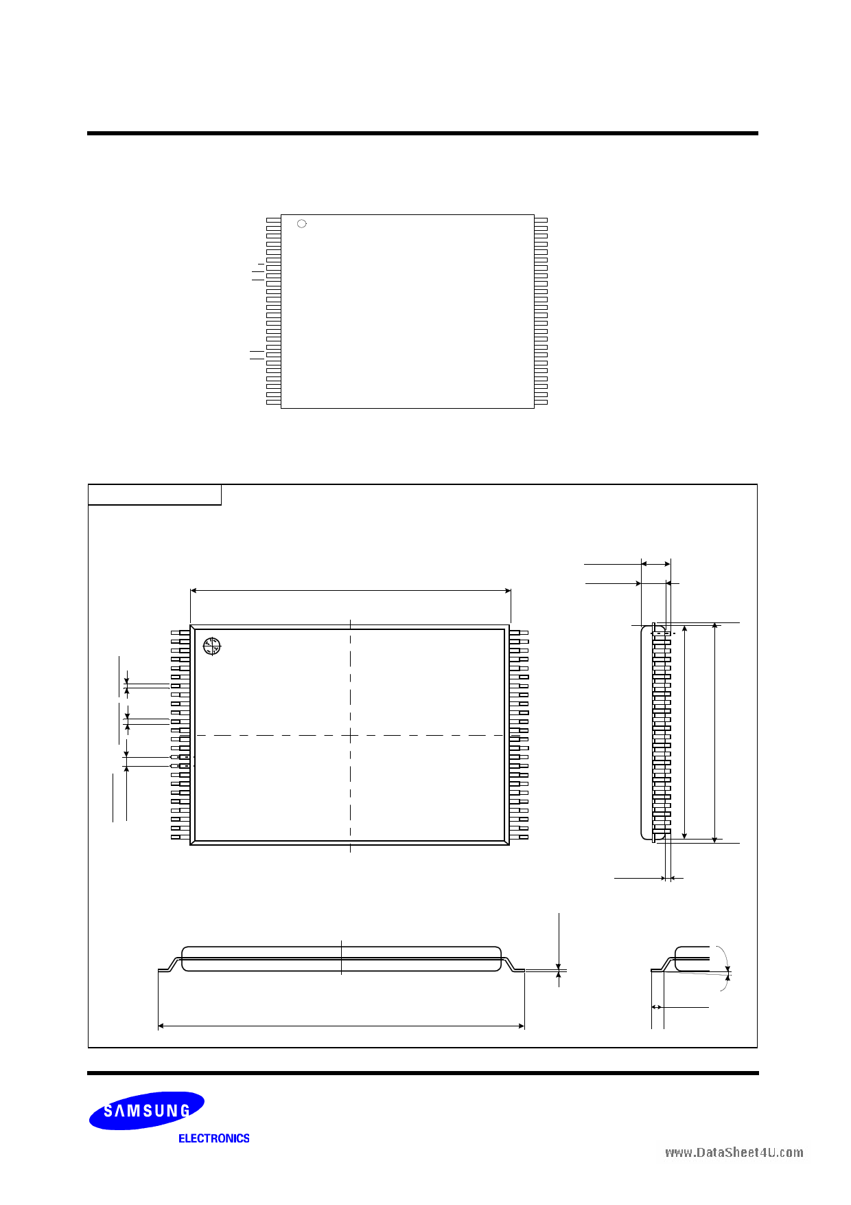
PIN CONFIGURATION (WSOP1)
K9F1208U0A-VCB0,FCB0/VIB0,FIB0
N.C
N.C
DNU
N.C
N.C
N.C
R/B
RE
CE
DNU
N.C
Vcc
Vss
N.C
DNU
CLE
ALE
WE
WP
N.C
N.C
DNU
N.C
N.C
1
2
3
4
5
6
7
8
9
10
11
12
13
14
15
16
17
18
19
20
21
22
23
24
48 N.C
47 N.C
46 DNU
45 N.C
44 I/O7
43 I/O6
42 I/O5
41 I/O4
40 N.C
39 DNU
38 N.C
37 Vcc
36 Vss
35 N.C
34 DNU
33 N.C
32 I/O3
31 I/O2
30 I/O1
29 I/O0
28 N.C
27 DNU
26 N.C
25 N.C
PACKAGE DIMENSIONS
48-PIN LEAD PLASTIC VERY VERY THIN SMALL OUT-LINE PACKAGE TYPE (I)
48 - WSOP1 - 1217F
Unit :mm
15.40±0.10
0.70 MAX
0.58±0.04
#1 #48
#24 #25
(0.01Min)
17.00±0.20
5
0.45~0.75
5 Page 
www.DataSheet4U.com
K9F1208D0A K9F1216D0A
K9F1208U0A K9F1216U0A
FLASH MEMORY
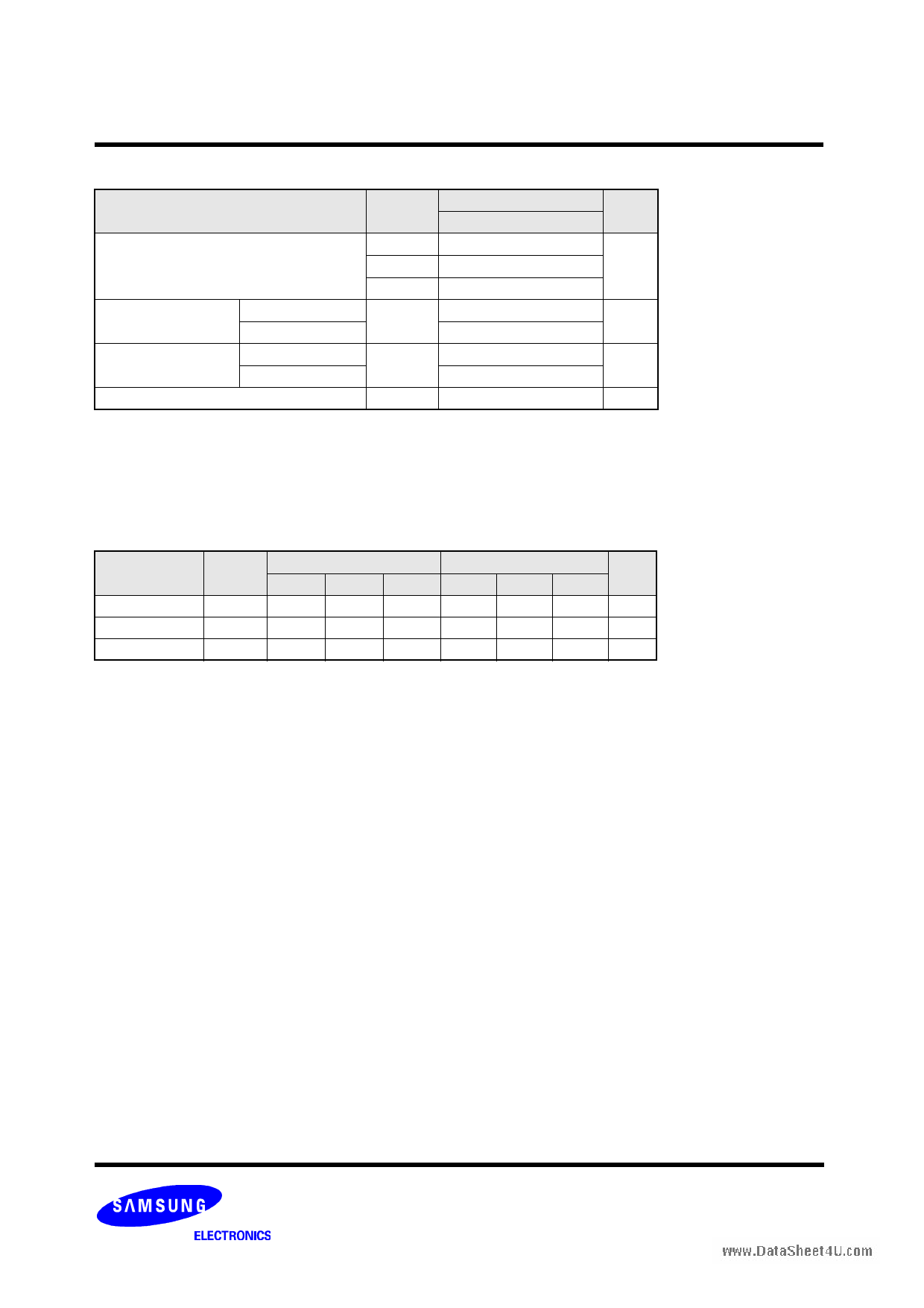
ABSOLUTE MAXIMUM RATINGS
Parameter
Symbol
Voltage on any pin relative to VSS
K9F12XXX0A-XCB0
Temperature Under Bias
K9F12XXX0A-XIB0
Storage Temperature
K9F12XXX0A-XCB0
K9F12XXX0A-XIB0
Short Circuit Current
VIN/OUT
VCC
VCCQ
TBIAS
TSTG
Ios
Rating
3.3V/2.65V DEVICE
-0.6 to + 4.6
-0.6 to + 4.6
-0.6 to + 4.6
Unit
V
°C
°C
mA
NOTE :
1. Minimum DC voltage is -0.6V on input/output pins. During transitions, this level may undershoot to -2.0V for periods <30ns.
Maximum DC voltage on input/output pins is VCC,+0.3V which, during transitions, may overshoot to VCC+2.0V for periods <20ns.
2. Permanent device damage may occur if ABSOLUTE MAXIMUM RATINGS are exceeded. Functional operation should be restricted to the conditions
as detailed in the operational sections of this data sheet. Exposure to absolute maximum rating conditions for extended periods may affect reliability.
RECOMMENDED OPERATING CONDITIONS
(Voltage reference to GND, K9F12XXX0A-XCB0 :TA=0 to 70°C, K9F12XXX0A-XIB0:TA=-40 to 85°C)
Parameter
Symbol
K9F12XXD0A(2.65V)
Min Typ. Max
K9F12XXU0A(3.3V)
Min Typ. Max
Unit
Supply Voltage
VCC
2.4 2.65 2.9
2.7 3.3
3.6
V
Supply Voltage
VCCQ
2.4 2.65 2.9
2.7
3.3
3.6
V
Supply Voltage
VSS
0
0
0
0
0
0V
11
11 Page | ||
| Páginas | Total 30 Páginas | |
| PDF Descargar | [ Datasheet K9F1208U0A.PDF ] | |
Hoja de datos destacado
| Número de pieza | Descripción | Fabricantes |
| K9F1208U0 | 64M x 8 Bit NAND Flash Memory | Samsung semiconductor |
| K9F1208U0A | (K9F1208x0A / K9F1216x0A) 64M x 8 Bit / 32M x 16 Bit NAND Flash Memory | Samsung semiconductor |
| K9F1208U0B | 64M x 8 Bit NAND Flash Memory | Samsung semiconductor |
| K9F1208U0B | 64M x 8 Bit NAND Flash Memory | Samsung semiconductor |
| Número de pieza | Descripción | Fabricantes |
| SLA6805M | High Voltage 3 phase Motor Driver IC. |
Sanken |
| SDC1742 | 12- and 14-Bit Hybrid Synchro / Resolver-to-Digital Converters. |
Analog Devices |
|
DataSheet.es es una pagina web que funciona como un repositorio de manuales o hoja de datos de muchos de los productos más populares, |
| DataSheet.es | 2020 | Privacy Policy | Contacto | Buscar |
