|
|
|
PDF PL610-01 Data sheet ( Hoja de datos )
| Número de pieza | PL610-01 | |
| Descripción | 1MHz to 130MHz XO IC | |
| Fabricantes | PhaseLink Corporation | |
| Logotipo | ||
Hay una vista previa y un enlace de descarga de PL610-01 (archivo pdf) en la parte inferior de esta página. Total 11 Páginas | ||
|
No Preview Available !
P(Preliminary) L610-01
1.8V to 3.3V, 1MHz to 130MHz XO IC
FEATURES
Wide frequency coverage, programmable, advanced
oscillator design.
Programmable “Odd/Even” Divider up to ÷63
Direct oscillation operation with optional
programmable features:
o Output Drive Strength (4, 8, or 16mA)
o 6-bit Odd/Even Output Divider
www.DataSheet4UIn.cpoumt Frequency:
o Fundamental Crystal: 5MHz to 130MHz
o Reference Clock: 1MHz to 130MHz
Supports CMOS or Sine Wave input clock
Output Frequency: 20kHz to 130MHz
Very low Jitter and Phase Noise
Low current consumption
Single 1.8V, 2.5V, or 3.3V ± 10% power supply
Operating temperature range from -40C to 85C
DESCRIPTION
The PL610 is a high performance general purpose
oscillator IC for outputs up to 130MHz. Designed to
fit in a small 2 x 1.3mm DFN or 3 x 3mm SOT23
package, the PL610 offers the best phase noise and
jitter performance and lowest power consumption of
any comparable IC.
In addition, there is a ‘6’ bit optional programmable
Odd/Even divider (default= ٪1), and ‘3’
programmable output drive strengths (4mA, 8mA
(default), 16mA) to choose from. The full feature set
of the PL610 makes it the most versatile XO for any
application.
PACKAGE PIN CONFIGURATION
XIN, FIN 1
6 XOUT
OE^, PDB^, CLK1 2
5 VDD
GND 3
4 CLK0
DFN-6L
(2.0mmx1.3mmx0.6mm)
OE^, PDB^, CLK1 1
6 CLK0
GND 2
5 VDD
XIN, FIN 3
4 XOUT
SOT23-6L
(3.0mmx3.0mmx1.35mm)
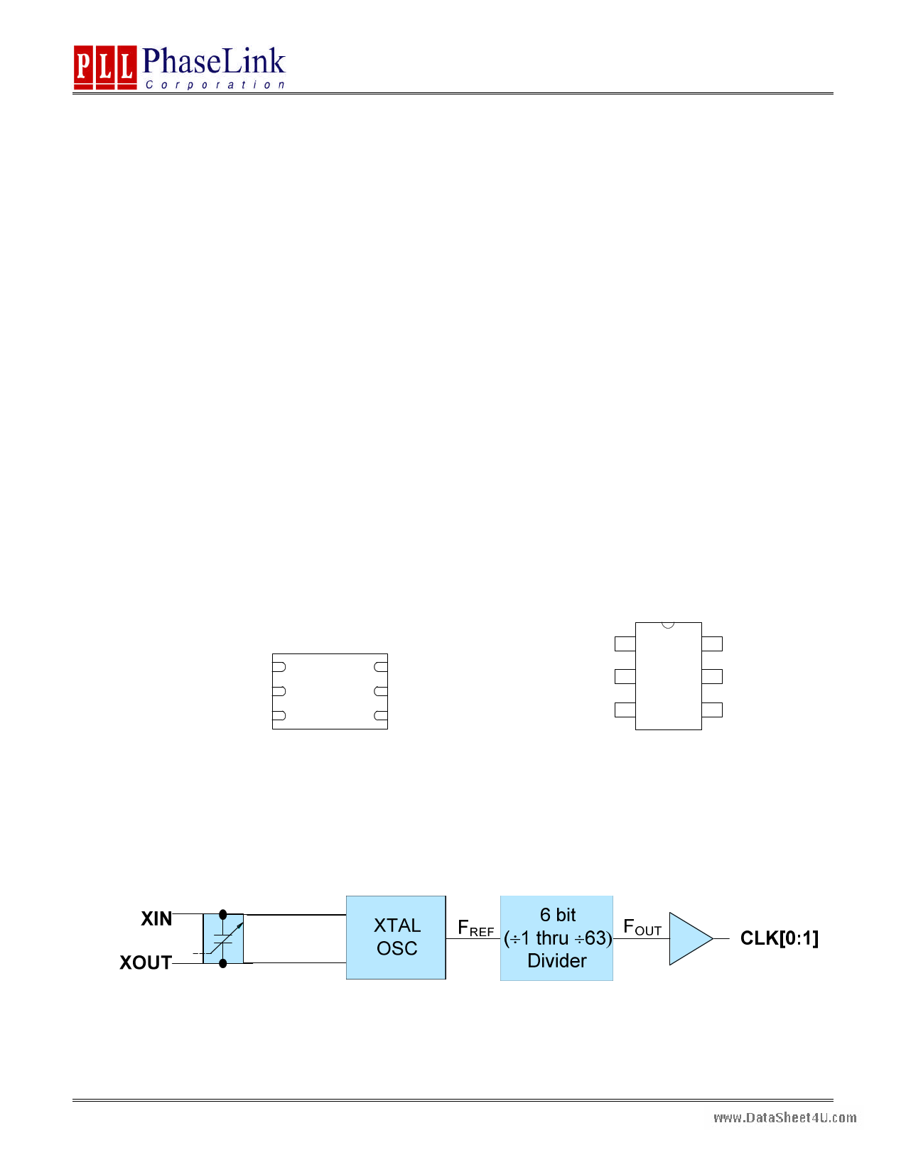
BLOCK DIAGRAM
47745 Fremont Blvd., Fremont, California 94538 Tel (510) 492-0990 Fax (510) 492-0991 www.phaselink.com Rev 4/2/07 Page 1
1 page 
P(Preliminary) L610-01
1.8V to 3.3V, 1MHz to 130MHz XO IC
ELECTRICAL SPECIFICATIONS
ABSOLUTE MAXIMUM RATINGS
PARAMETERS
SYMBOL
MIN.
MAX.
UNITS
Supply Voltage Range
VDD -0.5 4.6
V
Input Voltage Range
VI
-0.5 VDD+0.5
V
Output Voltage Range
www.DataSheetS4tUo.craomge Temperature
VO
-0.5 VDD+0.5
V
TS -65 150 C
Ambient Operating Temperature*
-40 85 C
Exposure of the device under conditions beyond the limits specified by Maximum Ratings for extended periods may cause permanent damage to the device
and affect product reliability. These conditions represent a stress rating only, and functional operations of the device at these or any other conditions above
the operational limits noted in this specification is not implied. *Operating temperature is guaranteed by design. Parts are tested to commercial grade only.
AC SPECIFICATIONS
PARAMETERS
CONDITIONS
MIN. TYP. MAX. UNITS
Crystal Input Frequency
Input (FIN) Frequency
Input (FIN) Signal Amplitude
Input (FIN) Signal Amplitude
Output Frequency
VDD Sensitivity
Output Rise Time
(See MTC-1)
Output Fall Time
(See MTC-1)
Duty Cycle
(See MTC-1)
Fundamental Crystal
@ VDD =3.3V
@ VDD =2.5V
@ VDD =1.8V
Internally AC coupled (High Frequency)
Internally AC coupled (Low Frequency)
3.3V <50MHz, 2.5V <40MHz, 1.8V <15MHz
@ Vdd=1.8V-3.3V
Frequency vs. VDD+/-10%
15pF Load, 10/90%VDD, High Drive, 3.3V
15pF Load, 90/10%VDD, High Drive, 3.3V
5
1
0.9
0.1
20kHz
-2
45
1
1
50
130 MHz
130 MHz
VDD Vpp
VDD Vpp
130 MHz
2 ppm
1.2 ns
1.2 ns
55 %
47745 Fremont Blvd., Fremont, California 94538 Tel (510) 492-0990 Fax (510) 492-0991 www.phaselink.com Rev 4/2/07 Page 5
5 Page 
P(Preliminary) L610-01
1.8V to 3.3V, 1MHz to 130MHz XO IC
ORDERING INFORMATION (GREEN PACKAGE)
www.DataSheet4U.com
For part ordering, please contact our Sales Department:
47745 Fremont Blvd., Fremont, CA 94538, USA
Tel: (510) 492-0990 Fax: (510) 492-0991
PART NUMBER
The order number for this device is a combination of the following:
Part number, Package type and Operating temperature range
PL610-01-XXX X X X
PART NUMBER
3 DIGIT ID Code *
(will be assigned at
programming time)
PACKAGE TYPE
T=SOT23-6L
G=DFN-6L
NONE= TUBE
R=TAPE and REEL
TEMPERATURE
C=COMMERCIAL
I=INDUSTRIAL
Part/Order Number
Marking†
Package Option
PL610-01-XXXGC-R
XXX 6-Pin DFN (Tape and Reel)
PL610-01-XXXTC-R
E1XXX
6-Pin SOT-23 (Tape and Reel)
† Note: ‘XXX’ designates marking identifier that could be independent of the part number.
PhaseLink Corporation, reserves the right to make changes in its products or specifications, or both at any time without notice. The information
furnished by Phaselink is believed to be accurate and reliable. However, PhaseLink makes no guarantee or warranty concerning the accuracy of said
information and shall not be responsible for any loss or damage of whatever nature resulting from the use of, or reliance upon this product.
LIFE SUPPORT POLICY: PhaseLink’s products are not authorized for use as critical components in life support devices or systems without the
express written approval of the President of PhaseLink Corporation.
Solder reflow profile available at www.phaselink.com/QA/solderingGreen.pdf
47745 Fremont Blvd., Fremont, California 94538 Tel (510) 492-0990 Fax (510) 492-0991 www.phaselink.com Rev 4/2/07 Page 11
11 Page | ||
| Páginas | Total 11 Páginas | |
| PDF Descargar | [ Datasheet PL610-01.PDF ] | |
Hoja de datos destacado
| Número de pieza | Descripción | Fabricantes |
| PL610-01 | Single IC XO | Microchip |
| PL610-01 | 1MHz to 130MHz XO IC | PhaseLink Corporation |
| PL610-01 | 1MHz to 130MHz XO IC | Micrel |
| PL610-02 | Single IC XO | Microchip |
| Número de pieza | Descripción | Fabricantes |
| SLA6805M | High Voltage 3 phase Motor Driver IC. |
Sanken |
| SDC1742 | 12- and 14-Bit Hybrid Synchro / Resolver-to-Digital Converters. |
Analog Devices |
|
DataSheet.es es una pagina web que funciona como un repositorio de manuales o hoja de datos de muchos de los productos más populares, |
| DataSheet.es | 2020 | Privacy Policy | Contacto | Buscar |