|
|
|
PDF PL611S-18 Data sheet ( Hoja de datos )
| Número de pieza | PL611S-18 | |
| Descripción | PicoPLLTM KHz to MHz Programmable Clock | |
| Fabricantes | PhaseLink Corporation | |
| Logotipo | ||
Hay una vista previa y un enlace de descarga de PL611S-18 (archivo pdf) en la parte inferior de esta página. Total 9 Páginas | ||
|
No Preview Available !
P(Preliminary) L611s-18
0.5kHz-125MHz MHz to KHz Programmable ClockTM
FEATURES
• Designed for Very Low-Power applications
• Offered in Tiny GREEN/RoHS compliant packages
o 6-pin DFN (2.0mmx1.3mmx0.6mm)
o 6-pin SC70 (2.3mmx2.25mmx1.0mm)
o 6-pin SOT23 (3.0mmx3.0mmx1.35mm)
• Accepts Crystal or Reference Clock inputs
• Input Frequency:
www.DataSheet4U.coomFundamental crystal: 10MHz to 50MHz
o Reference Input: 1MHz to 125MHz
• Accepts >0.1V reference signal input voltage
• Output Frequency 0.5kHz to 125MHz CMOS.
o 65MHz @ 1.8V operation
o 90MHz @ 2.5V operation
o 125MHz @ 3.3V operation
• One programmable I/O pin can be configured as
OE, PDB, FSEL or CLK1
• Low current consumption:
o <1.0mA with 27MHz & 32kHz outputs
o < 5µA when PDB is activated
• Single 1.8V, 2.5V, or 3.3V ± 10% power supply
• Operating temperature range from -40°C to 85°C
DESCRIPTION
The PL611s-18 is a low-cost general purpose
frequency synthesizer and a member of PhaseLink’s
PicoPLL family, the worlds smallest programmable
clocks. PhaseLink’s PL611s-18 offers the versatility
of using a single Crystal (MHz) or Reference Clock
input and producing up to two (kHz/MHz) system
clocks, or a combination of Reference and low
frequency outputs. The PL611s-18 is designed for
low-power applications with very stringent space
requirements and consumes ~1.0mA, while
producing 2 distinct outputs of 27MHz and 32kHz.
The power down feature of PL611s-18, when
activated, allows the IC to consume less than 5µA of
power.
The PL611s-18 fits in a small DFN, SC70, or SOT23
package. Cascading of the PL611s-18 with other
PhaseLink programmable clocks allow generating
system level clocking requirements, thereby
reducing the overall system implementation cost.
In addition, one programmable I/O pin can be
configured as Output Enable (OE), Frequency
switching (FSEL), Power Down (PDB) input, or CLK1
(CLK0, FREF, FREF/2) output.
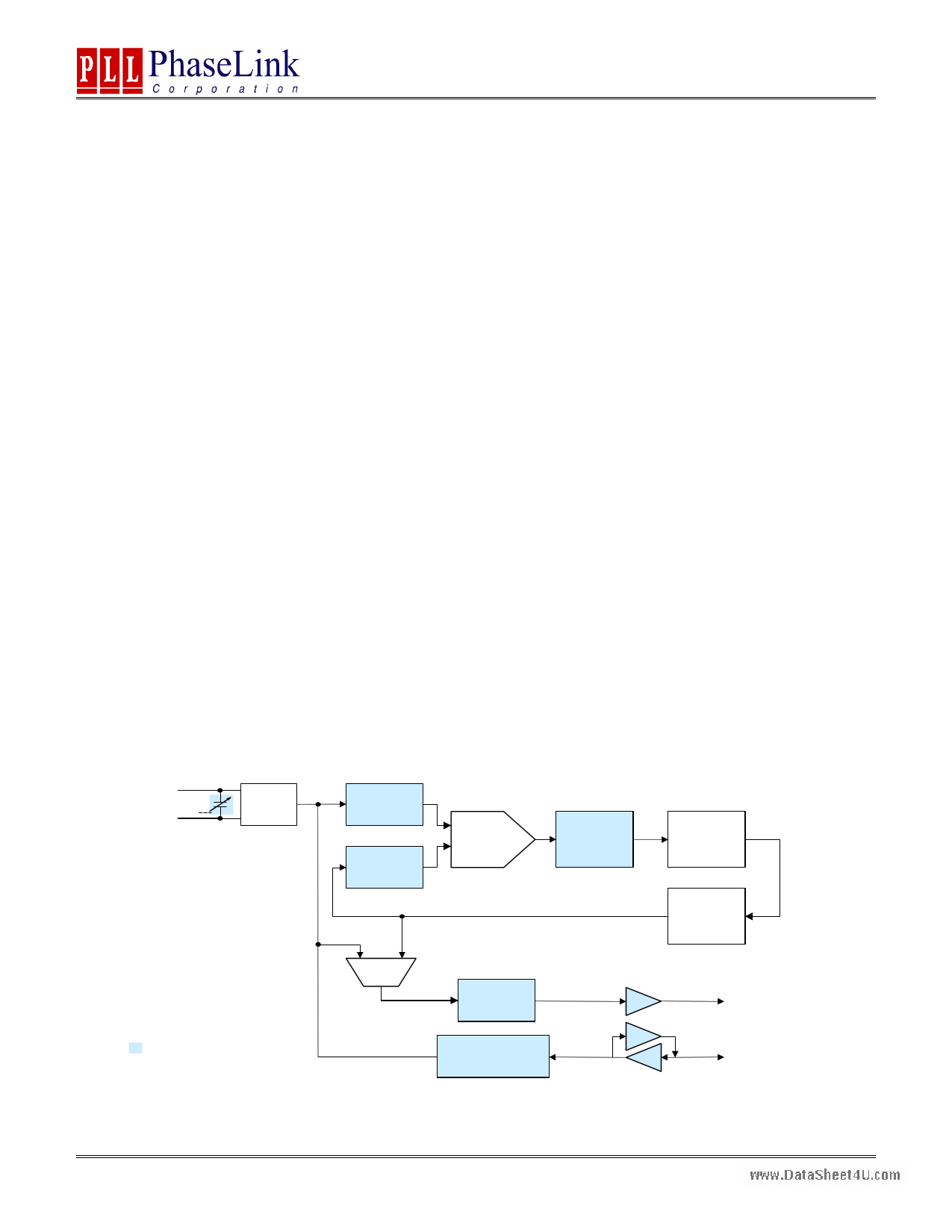
BLOCK DIAGRAM
XIN/FIN
XOUT
XTAL
OSC
Programmable
CLoad
FREF
R-Counter
(5-bit)
M-Counter
(8-bit)
Phase
Detector
FVCO = FREF * (2 * M/R)
Charge
Pump
Loop
Filter
VCO
Programmable Function
P-Counter
FOUT = FVCO / ( 2 * P) (14-bit)
Programming
Logic
CLK
OE, PDB,
FSEL, CLK1
47745 Fremont Blvd., Fremont, California 94538 Tel (510) 492-0990 Fax (510) 492-0991 www.phaselink.com Rev 2/23/07 Page 1
1 page 
P(Preliminary) L611s-18
0.5kHz-125MHz MHz to KHz Programmable ClockTM
DC SPECIFICATIONS
PARAMETERS
SYMBOL
CONDITIONS
Supply Current, Dynamic, with
Loaded CMOS Outputs
IDD
@ VDD =3.3V, 27MHz,
load=15pF
Supply Current, Dynamic, with
Loaded CMOS Outputs
IDD
@ VDD =2.5V, 27MHz,
load=10pF
Supply Current, Dynamic with
Loaded CMOS Outputs
IDD
@ VDD =1.8V, 27MHz,
load=5pF
www.DataSheePt4LUL.cOomff: Supply Current, Dynamic,
with Loaded CMOS Output
IDD
@ VDD =3.3V, 27MHz,
load=15pF
PLL Off: Supply Current, Dynamic,
with Loaded CMOS Output
IDD
@ VDD =2.5V, 27MHz,
load=10pF
PLL Off: Supply Current, Dynamic
with Loaded CMOS Output
IDD
@ VDD =1.8V, 27MHz,
load=5pF
PLL Off: Supply Current, Dynamic
with Loaded CMOS Output
IDD
@ VDD =1.8V, 32kHz,
load=5pF
Supply Current, Dynamic, with
Loaded Outputs
IDD When PDB=0
Operating Voltage
VDD
Output Low Voltage
VOL IOL = +4mA Standard Drive
Output High Voltage
VOH IOH = -4mA Standard Drive
Output Current, Low Drive
IOSD VOL = 0.4V, VOH = 2.4V
Output Current, Standard Drive
IOSD VOL = 0.4V, VOH = 2.4V
Output Current, High Drive
IOHD VOL = 0.4V, VOH = 2.4V
Short-Circuit Current
IS
* Note: Please contact PhaseLink, if super-low-power is required.
MIN.
1.62
VDD – 0.4
4
8
16
TYP.
4.0
2.7
0.9
2.0
1.3
0.8
0.2
±50
MAX.
5
3.63
0.4
UNITS
mA
mA
mA
mA
mA
mA
mA
µA
V
V
V
mA
mA
mA
mA
CRYSTAL SPECIFICATIONS
PARAMETERS
Fundamental Crystal Resonator Frequency
Crystal Loading Rating
(The IC can be programmed for any value in this range.)
Maximum Sustainable Drive Level
Operating Drive Level
Metal Can Crystal
Shunt Capacitance
ESR Max
Small SMD Crystal
Shunt Capacitance
ESR Max
SYMBOL
FXIN
CL (xtal)
C0
ESR
C0
ESR
MIN.
10
8
TYP.
30
MAX.
50
12
100
5.5
50
2.5
80
UNITS
MHz
pF
µW
µW
pF
Ω
pF
Ω
47745 Fremont Blvd., Fremont, California 94538 Tel (510) 492-0990 Fax (510) 492-0991 www.phaselink.com Rev 2/23/07 Page 5
5 Page | ||
| Páginas | Total 9 Páginas | |
| PDF Descargar | [ Datasheet PL611S-18.PDF ] | |
Hoja de datos destacado
| Número de pieza | Descripción | Fabricantes |
| PL611S-15 | PicoPLLTM 32K Programmable Clock | PhaseLink Corporation |
| PL611S-15 | PicoPLLTM 32K Programmable Clock | PhaseLink Corporation |
| PL611S-16 | PicoPLLTM 32K Programmable Clock | PhaseLink Corporation |
| PL611S-17 | PicoPLLTM KHz to MHz Programmable Clock | PhaseLink Corporation |
| Número de pieza | Descripción | Fabricantes |
| SLA6805M | High Voltage 3 phase Motor Driver IC. |
Sanken |
| SDC1742 | 12- and 14-Bit Hybrid Synchro / Resolver-to-Digital Converters. |
Analog Devices |
|
DataSheet.es es una pagina web que funciona como un repositorio de manuales o hoja de datos de muchos de los productos más populares, |
| DataSheet.es | 2020 | Privacy Policy | Contacto | Buscar |