|
|
|
PDF OL2068 Data sheet ( Hoja de datos )
| Número de pieza | OL2068 | |
| Descripción | Industrial 30 Volt 4-Channel Differential Power Line Driver | |
| Fabricantes | Optolab | |
| Logotipo | ||
Hay una vista previa y un enlace de descarga de OL2068 (archivo pdf) en la parte inferior de esta página. Total 9 Páginas | ||
|
No Preview Available !
OL2068
Industrial 30 Volt 4-Channel Differential Power Line Driver - Short Circuit Proof -
Applications
• Industrial encoder interfacing
• Industrial sensor interfacing
• Proximity switches
• Industrial controllers
• Light barriers
www.DataSheet4U.com
Features
· Ultra small package TSSOP 20
· Max. voltage range from 4,5 V – 36 V
· Short circuit proof tri-state outputs drive up to 120mA
sink / source
· Operating frequency up to 4 MHz
· Integrated voltage reg. with 5V output
· Dynamic peak current up to 1,5 Amp.
· High impedance CMOS / TTL compatible buffered
inputs with hysteresis
· Outputs RS422A compatible
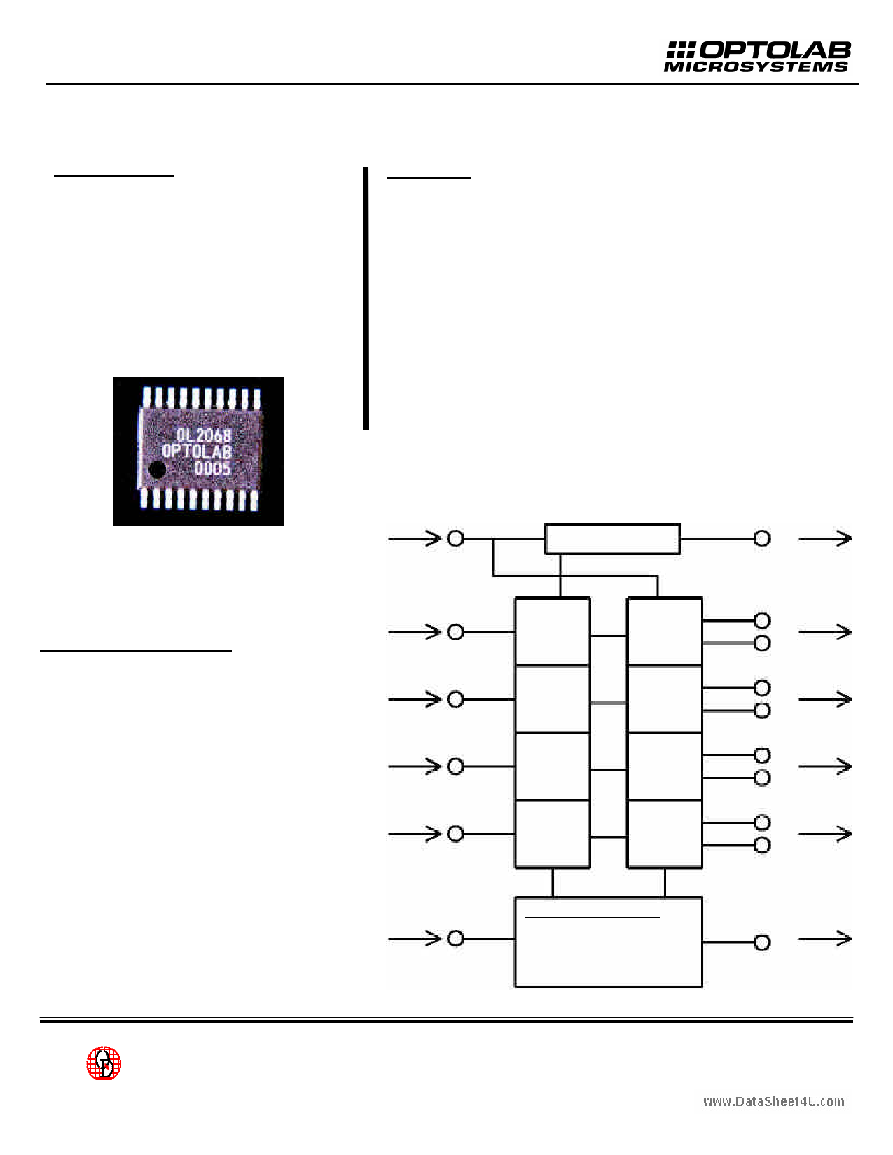
Ultra small package TSSOP 20
Line voltage in
Voltage regulator
5V , 5mA out
General Description
CMOS / TTL
Data input
Differential
Output A
Output A-
The OL2068 is an industrial power line
driver and contains four identical short cir-
cuit proof differential line drivers up to 30
Volts driver supply with a joint enable func-
tion. An internal 5 V power supply is used
as reference and supply voltage for the
circuitry and is able to supply max. 5mA
for external 5V components like a sensor
or a constant current source for an LED.
The very small outline TSSOP package
gives excellent thermal power dissipation,
thus the usage in space limited applica-
tions is easy.
Tristate enable / disable
Thermal shutdown disable
CMOS / TTL
Data input
CMOS / TTL
Data input
CMOS / TTL
Data input
Differential
Output B
Output B-
Differential
Output C
Output C-
Differential
Output D
Output D-
Protection logic controller
- short circuit shut down
- Tristate and thermal logic control
- Undervoltage and power up reset
- Transient and EMI protection
Error signal out
For Stateside information contact...
Quantum Devices, Inc., 112 Orbison St., PO Box 100, Barneveld, WI, 53507
1 page 
OL2068
Industrial 30 Volt 4-Channel Differential Power Line Driver - Short Circuit Proof -
Mechanical characteristics
Package Dimensions
Symbol
TSSOP20(173 mil)
Min Typ Max
D 6.40(0,25)
-
6.60(0,26)
E1 4.30(0,17)
-
www.DataSheet4U.com
E-
6.40(0,25)
4.50(0,18)
-
A-
- 1.20(47)
A1 0.05(2)
-
0.15(6)
b 0.19(7) - 0.30(11)
e - 0.65(26) -
L 0.50(20)
-
0.75(30)
α-
8
-
Unit
mm(inch)
mm(inch)
mm(inch)
mm(mils)
mm(mils)
mm(mils)
mm(mils)
mm(mils)
o
Form of delivery and order code
TSSOP20
Antistatic tubes containing 70pcs order part no. OL2068
Tape & Reel part no. OL2068 TR
High thermal power dissipation by integrated heatlink append “HL” to part number.
A demoboard with 2 line drivers plus connectors and status LEDs is available with order code
OL2068 Demo
Notes:
For hybrid applications this driver is also available as chip. Please contact us for further details.
For space critical applications custom design packages, i.e. with 2 or more driver chips in one package, can
be designed at customer request. Please email Quantum Devices, Inc. at [email protected]
For Stateside information contact...
Quantum Devices, Inc., 112 Orbison St., PO Box 100, Barneveld, WI, 53507
5 Page | ||
| Páginas | Total 9 Páginas | |
| PDF Descargar | [ Datasheet OL2068.PDF ] | |
Hoja de datos destacado
| Número de pieza | Descripción | Fabricantes |
| OL2068 | Industrial 30 Volt 4-Channel Differential Power Line Driver | Optolab |
| Número de pieza | Descripción | Fabricantes |
| SLA6805M | High Voltage 3 phase Motor Driver IC. |
Sanken |
| SDC1742 | 12- and 14-Bit Hybrid Synchro / Resolver-to-Digital Converters. |
Analog Devices |
|
DataSheet.es es una pagina web que funciona como un repositorio de manuales o hoja de datos de muchos de los productos más populares, |
| DataSheet.es | 2020 | Privacy Policy | Contacto | Buscar |