|
|
|
PDF CYWUSB6935 Data sheet ( Hoja de datos )
| Número de pieza | CYWUSB6935 | |
| Descripción | WirelessUSB LRTM 2.4-GHz DSSS Radio SoC | |
| Fabricantes | Cypress Semiconductor | |
| Logotipo | ||
Hay una vista previa y un enlace de descarga de CYWUSB6935 (archivo pdf) en la parte inferior de esta página. Total 30 Páginas | ||
|
No Preview Available !
CYWUSB6935
WirelessUSB LR™ 2.4-GHz DSSS Radio SoC
1.0 Features
• 2.4-GHz radio transceiver
• Operates in the unlicensed Industrial, Scientific, and
Medical (ISM) band (2.4 GHz–2.483 GHz)
• –95-dBm receive sensitivity
• Up to 0dBm output power
• Range of up to 50 meters or more
• Data throughput of up to 62.5 kbits/sec
www.DataSheet4•UH.ciogmhly integrated low cost, minimal number of external
components required
• Dual DSSS reconfigurable baseband correlators
• SPI microcontroller interface (up to 2-MHz data rate)
• 13-MHz input clock operation
• Low standby current < 1 µA
• Integrated 30-bit Manufacturing ID
• Operating voltage from 2.7V to 3.6V
• Operating temperature from –40° to 85°C
• Offered in a small footprint 48 QFN
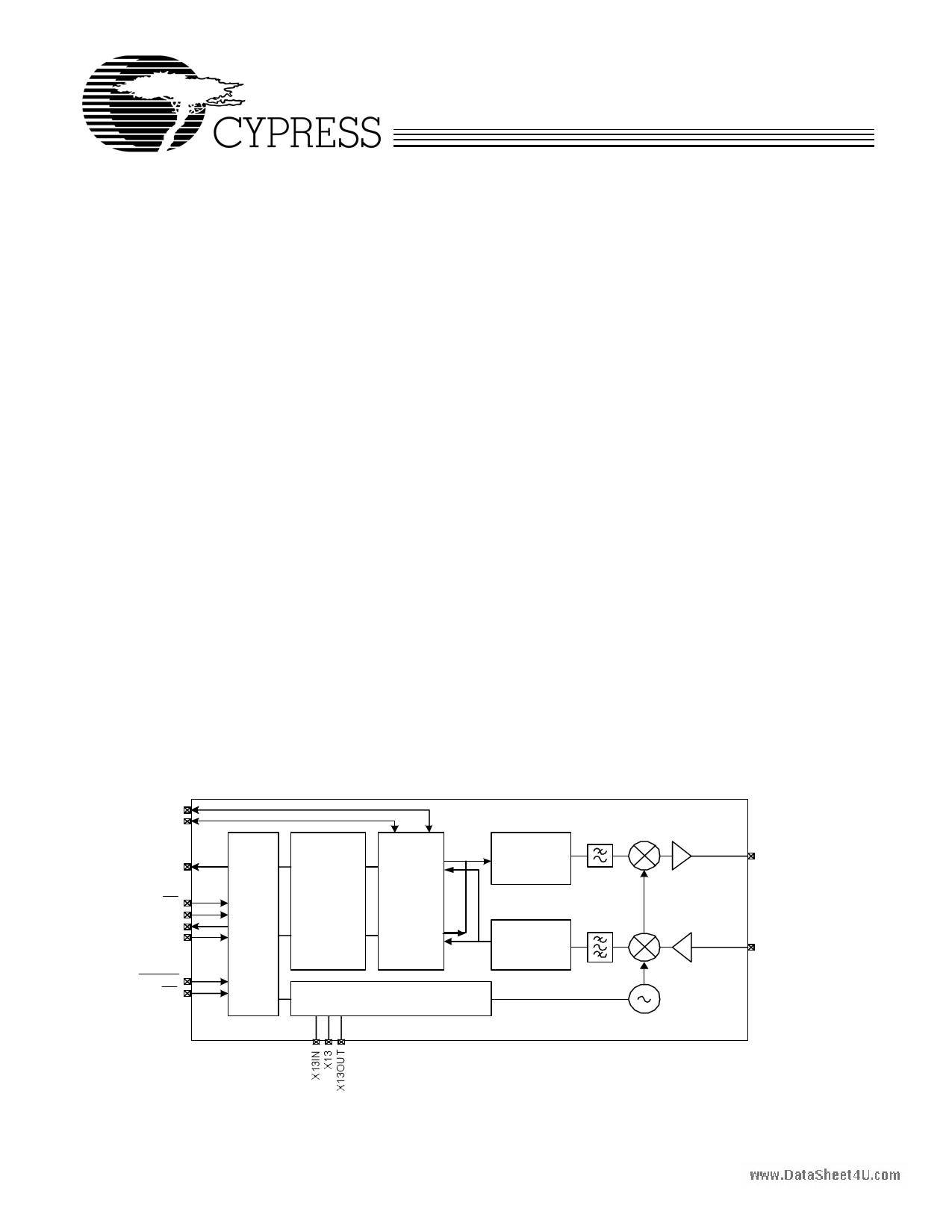
2.0 Functional Description
The CYWUSB6935 transceiver is a single-chip 2.4-GHz Direct
Sequence Spread Spectrum (DSSS) Gaussian Frequency
Shift Keying (GFSK) baseband modem radio that connects
directly to a microcontroller via a simple serial peripheral
interface.
The CYWUSB6935 is offered in an industrial temperature
range 48-pin QFN and a commercial temperature range 48-
pin QFN.
3.0 Applications
• Building/Home Automation
— Climate Control
— Lighting Control
— Smart Appliances
— On-Site Paging Systems
— Alarm and Security
• Industrial Control
— Inventory Management
— Factory Automation
— Data Acquisition
• Automatic Meter Reading (AMR)
• Transportation
— Diagnostics
— Remote Keyless Entry
• Consumer / PC
— Locator Alarms
— Presenter Tools
— Remote Controls
— Toys
DIOV A L
DIO
IRQ
SS
SCK
MISO
MOSI
RESET
PD
Digital
SERDES
A
DSSS
Bas eband
A
SERDES
B
DSSS
Bas eband
B
Synthesizer
GFSK
Modulator
GFSK
Demodulator
RFOUT
RFIN
Figure 3-1. CYWUSB6935 Simplified Block Diagram
Cypress Semiconductor Corporation
Document #: 38-16008 Rev. *C
• 3901 North First Street
• San Jose, CA 95134 • 408-943-2600
Revised March 17, 2005
1 page 
CYWUSB6935
5.2 DIO Interface
The DIO communications interface is an optional SERDES
bypass data-only transfer interface. In receive mode, DIO and
DIOVAL are valid after the falling edge of IRQ, which clocks
the data as shown in Figure 5-6. In transmit mode, DIO and
DIOVAL are sampled on the falling edge of the IRQ, which
clocks the data as shown in Figure 5-7. The application MCU
samples the DIO and DIOVAL on the rising edge of IRQ.
5.3 Interrupts
The CYWUSB6935 features three sets of interrupts: transmit,
received, and a wake interrupt. These interrupts all share a
single pin (IRQ), but can be independently enabled/disabled.
www.DataSheeItn4Ut.rcaonmsmit mode, all receive interrupts are automatically
disabled, and in receive mode all transmit interrupts are
automatically disabled. However, the contents of the enable
registers are preserved when switching between transmit and
receive modes.
Interrupts are enabled and the status read through 6 registers:
Receive Interrupt Enable (Reg 0x07), Receive Interrupt Status
(Reg 0x08), Transmit Interrupt Enable (Reg 0x0D), Transmit
Interrupt Status (Reg 0x0E), Wake Enable (Reg 0x1C), Wake
Status (Reg 0x1D).
If more than 1 interrupt is enabled at any time, it is necessary
to read the relevant interrupt status register to determine which
event caused the IRQ pin to assert. Even when a given
interrupt source is disabled, the status of the condition that
would otherwise cause an interrupt can be determined by
reading the appropriate interrupt status register. It is therefore
possible to use the devices without making use of the IRQ pin
at all. Firmware can poll the interrupt status register(s) to wait
for an event, rather than using the IRQ pin.
The polarity of all interrupts can be set by writing to the Config-
uration register (Reg 0x05), and it is possible to configure the
IRQ pin to be open drain (if active low) or open source (if active
high).
5.3.1 Wake Interrupt
When the PD pin is low, the oscillator is stopped. After PD is
deasserted, the oscillator takes time to start, and until it has
done so, it is not safe to use the SPI interface. The wake
interrupt indicates that the oscillator has started, and that the
device is ready to receive SPI transfers.
The wake interrupt is enabled by setting bit 0 of the Wake
Enable register (Reg 0x1C, bit 0=1). Whether or not a wake
interrupt is pending is indicated by the state of bit 0 of the Wake
Status register (Reg 0x1D, bit 0). Reading the Wake Status
register (Reg 0x1D) clears the interrupt.
5.3.2 Transmit Interrupts
Four interrupts are provided to flag the occurrence of transmit
events. The interrupts are enabled by writing to the Transmit
Interrupt Enable register (Reg 0x0D), and their status may be
determined by reading the Transmit Interrupt Status register
(Reg 0x0E). If more than 1 interrupt is enabled, it is necessary
to read the Transmit Interrupt Status register (Reg 0x0E) to
determine which event caused the IRQ pin to assert.
The function and operation of these interrupts are described in
detail in Section 7.0.
5.3.3 Receive Interrupts
Eight interrupts are provided to flag the occurrence of receive
events, four each for SERDES A and B. In 64 chips/bit and 32
chips/bit DDR modes, only the SERDES A interrupts are
available, and the SERDES B interrupts will never trigger,
even if enabled. The interrupts are enabled by writing to the
Receive Interrupt Enable register (Reg 0x07), and their status
may be determined by reading the Receive Interrupt Status
register (Reg 0x08). If more than one interrupt is enabled, it is
necessary to read the Receive Interrupt Status register (Reg
0x08) to determine which event caused the IRQ pin to assert.
The function and operation of these interrupts are described in
detail in Section 7.0.
IRQ
DIOVAL
DIO
IRQ
DIOVAL
DIO
v0 v1 v2 v3 v4 v5 v6 v7 v8 v9 v10 v11 v12 v13 v14 v...
data to mcu
d0 d1 d2 d3 d4 d5 d6 d7 d8 d9 d10 d11 d12 d13 d14 d...
Figure 5-6. DIO Receive Sequence
v0 v1 v2 v3 v4 v5 v6 v7 v8 v9 v10 v11 v12 v13 v14 v...
data from mcu
d0 d1 d2 d3 d4 d5 d6 d7 d8 d9 d10 d11 d12 d13 d14 d...
Figure 5-7. DIO Transmit Sequence
Document #: 38-16008 Rev. *C
Page 5 of 33
5 Page 
CYWUSB6935
Addr: 0x07
76
Underflow B
Overflow B
REG_RX_INT_EN
5432
EOF B
Full B
Underflow A
Overflow A
Figure 7-6. Receive SERDES Interrupt Enable
Default: 0x00
10
EOF A
Full A
Bit Name
7 Underflow B
www.DataSheet64U.coOmverflow B
5 EOF B
4 Full B
3 Underflow A
2 Overflow A
1 EOF A
0 Full A
Description
The Underflow B bit is used to enable the interrupt associated with an underflow condition with the Receive SERDES
Data B register (Reg 0x0B)
1 = Underflow B interrupt enabled for Receive SERDES Data B
0 = Underflow B interrupt disabled for Receive SERDES Data B
An underflow condition occurs when attempting to read the Receive SERDES Data B register (Reg 0x0B) when it is
empty.
The Overflow B bit is used to enable the interrupt associated with an overflow condition with the Receive SERDES
Data B register (Reg 0x0B)
1 = Overflow B interrupt enabled for Receive SERDES Data B
0 = Overflow B interrupt disabled for Receive SERDES Data B
An overflow condition occurs when new received data is written into the Receive SERDES Data B register (Reg
0x0B) before the prior data is read out.
The End of Frame B bit is used to enable the interrupt associated with the Channel B Receiver EOF condition.
1 = EOF B interrupt enabled for Channel B Receiver
0 = EOF B interrupt disabled for Channel B Receiver
The EOF IRQ asserts during an End of Frame condition. End of Frame conditions occur after at least one bit has
been detected, and then the number of invalid bits in the frame exceeds the number in the EOF length field. If 0 is
the EOF length, and EOF condition will occur at the first invalid bit after a valid reception. This IRQ is cleared by
reading the receive status register
The Full B bit is used to enable the interrupt associated with the Receive SERDES Data B register (Reg 0x0B) having
data placed in it.
1 = Full B interrupt enabled for Receive SERDES Data B
0 = Full B interrupt disabled for Receive SERDES Data B
A Full B condition occurs when data is transferred from the Channel B Receiver into the Receive SERDES Data B
register (Reg 0x0B). This could occur when a complete byte is received or when an EOF event occurs whether or
not a complete byte has been received.
The Underflow A bit is used to enable the interrupt associated with an underflow condition with the Receive SERDES
Data A register (Reg 0x09)
1 = Underflow A interrupt enabled for Receive SERDES Data A
0 = Underflow A interrupt disabled for Receive SERDES Data A
An underflow condition occurs when attempting to read the Receive SERDES Data A register (Reg 0x09) when it is
empty.
The Overflow A bit is used to enable the interrupt associated with an overflow condition with the Receive SERDES
Data A register (0x09)
1 = Overflow A interrupt enabled for Receive SERDES Data A
0 = Overflow A interrupt disabled for Receive SERDES Data A
An overflow condition occurs when new receive data is written into the Receive SERDES Data A register (Reg 0x09)
before the prior data is read out.
The End of Frame A bit is used to enable the interrupt associated with an End of Frame condition with the Channel
A Receiver.
1 = EOF A interrupt enabled for Channel A Receiver
0 = EOF A interrupt disabled for Channel A Receiver
The EOF IRQ asserts during an End of Frame condition. End of Frame conditions occur after at least one bit has
been detected, and then the number of invalid bits in a frame exceeds the number in the EOF length field. If 0 is the
EOF length, an EOF condition will occur at the first invalid bit after a valid reception. This IRQ is cleared by reading
the receive status register.
The Full A bit is used to enable the interrupt associated with the Receive SERDES Data A register (0x09) having
data written into it.
1 = Full A interrupt enabled for Receive SERDES Data A
0 = Full A interrupt disabled for Receive SERDES Data A
A Full A condition occurs when data is transferred from the Channel A Receiver into the Receive SERDES Data A
register (Reg 0x09). This could occur when a complete byte is received or when an EOF event occurs whether or
not a complete byte has been received.
Document #: 38-16008 Rev. *C
Page 11 of 33
11 Page | ||
| Páginas | Total 30 Páginas | |
| PDF Descargar | [ Datasheet CYWUSB6935.PDF ] | |
Hoja de datos destacado
| Número de pieza | Descripción | Fabricantes |
| CYWUSB6932 | WirelessUSB LS 2.4-GHz DSSS Radio SoC | Cypress Semiconductor |
| CYWUSB6932 | (CYWUSB6932 / CYWUSB6934) DSSS Radio SoC | Cypress Semiconductor |
| CYWUSB6932-48LFXC | WirelessUSB LS 2.4-GHz DSSS Radio SoC | Cypress Semiconductor |
| CYWUSB6934 | WirelessUSB LS 2.4-GHz DSSS Radio SoC | Cypress Semiconductor |
| Número de pieza | Descripción | Fabricantes |
| SLA6805M | High Voltage 3 phase Motor Driver IC. |
Sanken |
| SDC1742 | 12- and 14-Bit Hybrid Synchro / Resolver-to-Digital Converters. |
Analog Devices |
|
DataSheet.es es una pagina web que funciona como un repositorio de manuales o hoja de datos de muchos de los productos más populares, |
| DataSheet.es | 2020 | Privacy Policy | Contacto | Buscar |