|
|
|
PDF NJW4302 Data sheet ( Hoja de datos )
| Número de pieza | NJW4302 | |
| Descripción | THREE-PHASE DC BRUSHLESS MOTOR CONTROL IC | |
| Fabricantes | New Japan Radio | |
| Logotipo | ||
Hay una vista previa y un enlace de descarga de NJW4302 (archivo pdf) en la parte inferior de esta página. Total 18 Páginas | ||
|
No Preview Available !
NJW4302
THREE-PHASE DC BRUSHLESS MOTOR CONTROL IC
s GENERAL DESCRIPTION
The NJW4302 is a three-phase DC brushless motor
pre-driver IC for precision applications.
The NJW4302 consists of PWM driver, motor velocity
control, FG(Frequency Generator) output, and voltage
velocity integration circuit.
The NJW4302 realizes stabilized velocity and it is suitable
for printer, FAX, and other DC motor control systems.
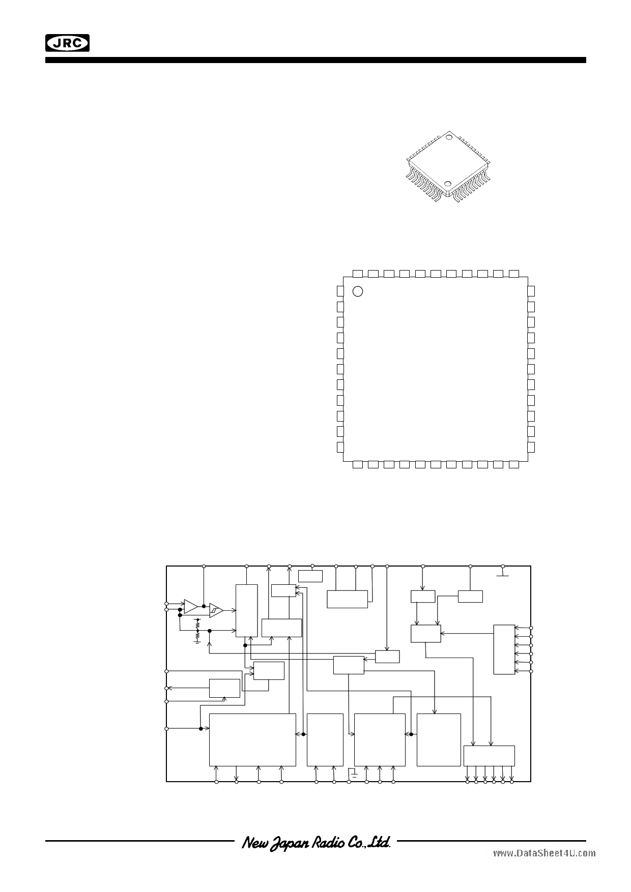
s PACKEGE OUTLINE
NJW4302FA1
Preliminary
•www.DataSheest4UF.EcoAmTURES
Speed discriminator and PLL speed
control circuit
• Direct PWM driver
• CR oscillator
•Lock protection output
•Break circuit (short circuit braking)
•Start/stop switch Start/Stop Switch Circuit
•Current limit circuit
•Thermal shut down/Under voltage
lockout circuit
•FG output amplifier/Integrating circuit
•Shunt regulator output : 5V
•Bi-CMOS technology
•PACKAGE OUTLINE QFP44
s PIN CONFIGRATION
WL VH VL UH UL RF H3 H3 H2 H2 H1
WH
PVCC
VCC
VREG
DGND
AGND
VSH
CR
CROCK
R
C
NJW4302 QFP44
H1+
FGIN+
FGIN-
FGOUT
FGSOUT
PGND
AGND
N2
N1
SS
CLK
sBLOCK DIAGRAM
FILO FILI
TOC
INT IN POUT LD BR FR
INTREF INTOUT DOUT
FGIN-
F G IN+
Pout
Vre g
VS H
CLK
FGO
-
+
-
+
FGSO D o ut
O
LD
LD
FG
C R OC K IN TR EFIN TIN IN TOU TS/S
ROCK
OSC
F
IN TEGR ATION
AMP
SPEED
D I SC RIMI N ATOR
VR EG 1
SPEED
PLL
VC OO U T
PLL COUNTER
VR EF
S /S
ALTER N ATIVE
C OU N TER
CIR CUIT
PWM BLOCK
BR F/R V+
B R F/R
L OGIC
H AL L
H YS
AMP
PR OTEC TION
C IR C U IT
TS D / L VD S
P R I- D R IVER
H1+
H1 -
H2+
H2 -
H3+
H3 -
FILI FILO
R
C
N1 N2 GND CR RF TOC
U L VL WL U H VH WH
-1-
1 page 
NJW4302
Preliminary
7. Brake Switch
NJW4302 uses a short brake method that turns on all phase of upper side transistors for braking. During the
time, all lower side transistors are turned off.
8. VREG pin/VSH pin
NJW4302 includes a regulator to generate for +5V regulated IC supply when the motor drive circuit
is designed with a single power supply. The VREG pin and V+ pin compose a shunt regulator for 5V±5%
output with a external resistor and a transistor. To use the regulator, the VSH pin must be either “H”, or Open.
Otherwise, the VSH pin must be “L” and the VREG pin is to be opened.
www.DataSh9e.et4FUr.ecoqmuency Generator (FG) Amplifier
The internal FG amplifier with few passive components composes a filter amplifier shown in the
application. Circuit for noise rejection. The output voltage of the amplifier must be at least 250mA p-p since it feature
Schmitt comparator.
The capacitor connected between the FGIN+ pin and the ground is necessary for bias voltage
stabilization and initial reset pulse generation for the internal logic. The reset pulse is generated when the
FGIN+ pin goes from 0 to approximately 1.25V.
10. Integration Amplifier
The integration amplifier integrates the D-out and P-out and converts them to speed command voltage. During the
time, it also sets the control loop gain and frequency characteristics using external components.
11. Speed Control Circuit
NJW4302 features two speed control method; speed discriminator circuit with PLL circuit and phase
comparison circuit. The FG pulse frequency is controlled to be the same frequency with a clock frequency input to the CLK
pin. Therefore, the motor speed can be controlled by changing the clock frequency.
The motor speed (N) can be expressed as:
N=CLK (Hz)×(60/FGP)[RPM] ( FGP: Number of FG pulse per one rotation)
Given that the oscillation frequency range is 160kHz~1.0MHZ and the number of counts is 1024,the range of
clock frequency is 156HZ~960HZ,and therefore the motor speed can be changed from 260rpm to 1600rpm.
-5-
5 Page 
s SPEED DISCRIMINATOR COUNT TABLE
N1 N2
High or Open
High or Open
High or Open
Low
Low High or Open
Low Low
NUMBER OF COUNTS
128
512
256
1024
s THREE PHASE LOGIC TRUTH TABLE
www.DataSheet4U.com
F/R=L
F/R=H
OUTPUTS
H 1 H 2 H 3 H 1 H 2 H 3 Source Sink
1 H L H L H L VH UL
2 H L L L H H WH UL
3 H H L L L H WH VL
4 L H L H L H UH VL
5 L H H H L L UH WL
6 L L H H H L VH WL
s S/S TERMINAL
High or Open
Low
Stop
Start
s BRAKE TERMINAL
High or Open
Low
Brake
Release
NJW4302
Preliminary
- 11 -
11 Page | ||
| Páginas | Total 18 Páginas | |
| PDF Descargar | [ Datasheet NJW4302.PDF ] | |
Hoja de datos destacado
| Número de pieza | Descripción | Fabricantes |
| NJW4301 | 2 CHANNEL BRIDGE DRIVER IC | New Japan Radio |
| NJW4302 | THREE-PHASE DC BRUSHLESS MOTOR CONTROL IC | New Japan Radio |
| NJW4303 | PWM 3-PHASE DC BRUSHLESS MOTOR CONTROLLER | New Japan Radio |
| NJW4305A | 3 PHASE BRUSHLESS DC MOTOR CONTROLL IC | New Japan Radio |
| Número de pieza | Descripción | Fabricantes |
| SLA6805M | High Voltage 3 phase Motor Driver IC. |
Sanken |
| SDC1742 | 12- and 14-Bit Hybrid Synchro / Resolver-to-Digital Converters. |
Analog Devices |
|
DataSheet.es es una pagina web que funciona como un repositorio de manuales o hoja de datos de muchos de los productos más populares, |
| DataSheet.es | 2020 | Privacy Policy | Contacto | Buscar |