|
|
PDF ATxMEGA256A1 Data sheet ( Hoja de datos )
| Número de pieza | ATxMEGA256A1 | |
| Descripción | (ATxMEGAxxxA1) 8/16-bit XMEGA A1 Microcontroller | |
| Fabricantes | ATMEL Corporation | |
| Logotipo |  |
|
Hay una vista previa y un enlace de descarga de ATxMEGA256A1 (archivo pdf) en la parte inferior de esta página. Total 30 Páginas | ||
|
No Preview Available !
Features
• High-performance, Low-power 8/16-bit AVR XMEGA Microcontroller
• Non-Volatile Program and Data Memories
– 64K - 384K Bytes of In-System Self-Programmable Flash
– 4K - 8K Bytes Boot Section with Independent Lock Bits
– 2K - 4K Bytes EEPROM
– 4K - 32K Bytes Internal SRAM
External Bus Interface for up to 16M bytes SRAM
External Bus Interface for up to 128M bit SDRAM
• Peripheral Features
– Four-channel DMA Controller with support for external requests
– Eight-channel Event System
– Eight 16-bit Timer/Counters
www.DataSheet4U.cFoomur Timer/Counters with 4 Output Compare or Input Capture channels
Four Timer/Counters with 2 Output Compare or Input Capture channels
High-Resolution Extension on all Timer/Counters
Advanced Waveform Extension on two Timer/Counters
– Eight USARTs
IrDA modulation/demodulation for one USART
– Four Two-Wire Interfaces with dual address match (I2C and SMBus compatible)
– Four SPI (Serial Peripheral Interface) peripherals
– AES and DES Crypto Engine
– 16-bit Real Time Counter with separate Oscillator
– Two Eight-channel, 12-bit, 2 Msps Analog to Digital Converters
– Two Two-channel, 12-bit, 1 Msps Digital to Analog Converters
– Four Analog Comparators with Window compare function
– External Interrupts on all General Purpose I/O pins
– Programmable Watchdog Timer with Separate On-chip Ultra Low Power Oscillator
• Special Microcontroller Features
– Power-on Reset and Programmable Brown-out Detection
– Internal and External Clock Options with PLL and Prescaler
– Programmable Multi-level Interrupt Controller
– Sleep Modes: Idle, Power-down, Standby, Power-save, Extended Standby
– Advanced Programming, Test and Debugging Interfaces
JTAG (IEEE 1149.1 Compliant) Interface for programming, test and debugging
PDI (Program and Debug Interface) for programming and debugging
• I/O and Packages
– 78 Programmable I/O Lines
– 100 - lead TQFP
– 100 - ball CBGA
• Operating Voltage
– 1.6 – 3.6V
• Speed performance
– 0 – 12 MHz @ 1.6 – 3.6V
– 0 – 32 MHz @ 2.7 – 3.6V
Typical Applications
• Industrial control
• Factory automation
• Climate control
• ZigBee
• Building control
• Motor control
• Board control
• Networking
• White Goods
• Optical
• Hand-held battery applications
• Power tools
• HVAC
• Metering
• Medical Applications
8/16-bit
XMEGA A1
Microcontroller
ATxmega384A1
ATxmega256A1
ATxmega192A1
ATxmega128A1
ATxmega64A1
Preliminary
8067D–AVR–08/08
1 page 
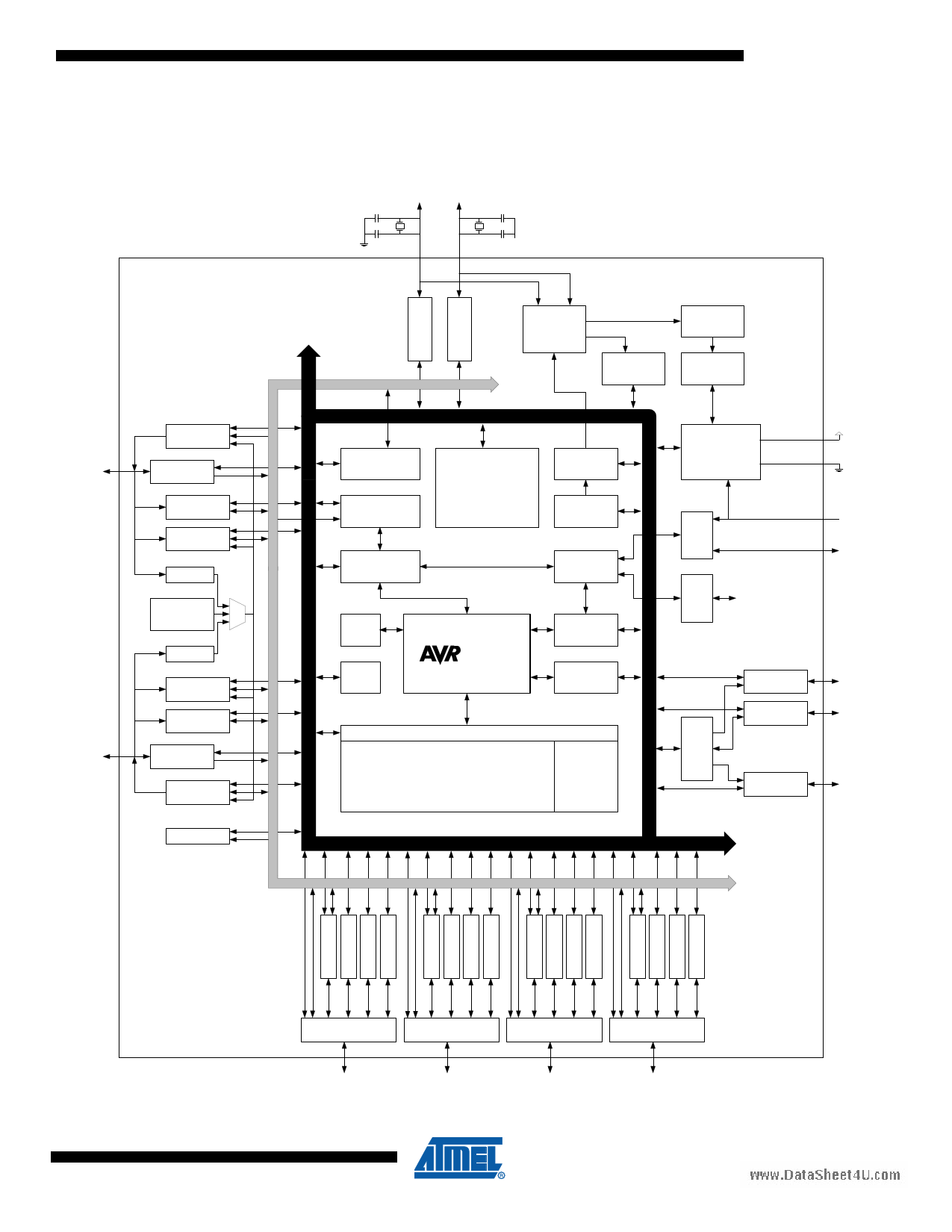
3.1 Block Diagram
Figure 3-1. XMEGA A1 Block Diagram
PR[0..1] PQ[0..3]
XTAL1
TOSC1
XTAL2
TOSC2
XMEGA A1
www.DataSheet4U.com
PA[0..7]
PB[0..7]/
JTAG
DACA
PORT A (8)
ACA
ADCA
AREFA
Internal
Reference
AREFB
ADCB
ACB
PORT B (8)
DACB
IRCOM
Oscillator
Circuits/
Clock
Generation
EVENT ROUTING NETWORK
DATA BUS
Real Time
Counter
Event System
Controller
DMA
Controller
SRAM
Oscillator
Control
Sleep
Controller
BUS
Controller
Prog/Debug
Controller
DES
AES
CPU
NVM Controller
Flash
OCD
Interrupt
Controller
EEPROM
Watchdog
Oscillator
Watchdog
Timer
Power
Supervision
POR/BOD &
RESET
PDI
JTAG
PORT B
PORT K (8)
PORT J (8)
EBI
PORT H (8)
VCC
GND
RESET/
PDI_CLK
PDI_DATA
PK[0..7]
PJ[0..7]
PH[0..7]
DATA BUS
EVENT ROUTING NETWORK
8067D–AVR–08/08
PORT C (8)
PC[0..7]
PORT D (8)
PD[0..7]
PORT E (8)
PE[0..7]
PORT F (8)
PF[0..7]
5
5 Page 
XMEGA A1
www.DataSheet4U.com
Byte Address
0
FFF
1000
1FFF
2000
9FFF
10000
FFFFFF
ATxmega384A1
I/O Registers
(4KB)
EEPROM
(4K)
Internal SRAM
(32K)
External Memory
(0 to 16 MB)
Byte Address
0
FFF
1000
1FFF
2000
5FFF
6000
FFFFFF
ATxmega256A1
I/O Registers
(4KB)
EEPROM
(4K)
Internal SRAM
(16K)
External Memory
(0 to 16 MB)
7.4.1
7.4.2
7.4.3
I/O Memory
All peripherals and modules are addressable through I/O memory locations in the data memory
space. All I/O memory locations can be accessed by the Load (LD/LDS/LDD) and Store
(ST/STS/STD) instructions, transferring data between the 32 general purpose registers in the
CPU and the I/O Memory.
The IN and OUT instructions can address I/O memory locations in the range 0x00 - 0x3F
directly.
I/O registers within the address range 0x00 - 0x1F are directly bit-accessible using the SBI and
CBI instructions. The value of single bits can be checked by using the SBIS and SBIC instruc-
tions on these registers.
The I/O memory address for all peripherals and modules in XMEGA A1 is shown in the “Periph-
eral Module Address Map” on page 54.
SRAM Data Memory
The XMEGA A1 devices has internal SRAM memory for data storage.
EEPROM Data Memory
The XMEGA A1 devices has internal EEPROM memory for non-volatile data storage. It is
addressable either in a separate data space or it can be memory mapped into the normal data
memory space. The EEPROM memory supports both byte and page access.
8067D–AVR–08/08
11
11 Page | ||
| Páginas | Total 30 Páginas | |
| PDF Descargar | [ Datasheet ATxMEGA256A1.PDF ] | |
Hoja de datos destacado
| Número de pieza | Descripción | Fabricantes |
| ATxMEGA256A1 | (ATxMEGAxxxA1) 8/16-bit XMEGA A1 Microcontroller | ATMEL Corporation |
| ATXMEGA256A3 | (ATXMEGAxxxA3) 8/16-bit XMEGA A3 Microcontroller | ATMEL Corporation |
| ATxmega256A3B | Microcontroller | ATMEL Corporation |
| ATxmega256A3BU | 8/16-bit Atmel XMEGA A3BUMicrocontroller | ATMEL Corporation |
| Número de pieza | Descripción | Fabricantes |
| SLA6805M | High Voltage 3 phase Motor Driver IC. |
Sanken |
| SDC1742 | 12- and 14-Bit Hybrid Synchro / Resolver-to-Digital Converters. |
Analog Devices |
|
DataSheet.es es una pagina web que funciona como un repositorio de manuales o hoja de datos de muchos de los productos más populares, |
| DataSheet.es | 2020 | Privacy Policy | Contacto | Buscar |
