|
|
|
PDF W3DG64126V-D2 Data sheet ( Hoja de datos )
| Número de pieza | W3DG64126V-D2 | |
| Descripción | SDRAM UNBUFFERED | |
| Fabricantes | White Electronic Designs | |
| Logotipo | ||
Hay una vista previa y un enlace de descarga de W3DG64126V-D2 (archivo pdf) en la parte inferior de esta página. Total 9 Páginas | ||
|
No Preview Available !
White Electronic Designs
W3DG64126V-D2
1GB – 2x64Mx64, SDRAM UNBUFFERED
FEATURES
PC100 and PC133 compatible
Burst Mode Operation
Auto and Self Refresh capability
LVTTL compatible inputs and outputs
Serial Presence Detect with EEPROM
Fully synchronous: All signals are registered on the
positive edge of the system clock
Programmable Burst Lengths: 1, 2, 4, 8 or Full Page
Available with "WP" write protect on pin 81 option
• W3DG63126V-D2
3.3V ± 0.3V Power Supply
168 Pin DIMM JEDEC
www.Data• SPhCeBe: t340U.5.0cmomm(1.20in)
DESCRIPTION
The W3DG64126V is a 2x64Mx64 synchronous DRAM
module which consists of sixteen 64Mx8 SDRAM
components in TSOP II package and one 2K EEPROM
in an 8 Pin TSSOP package for Serial Presence Detect
which are mounted on a 168 Pin DIMM multilayer FR4
Substrate.
* This product is subject to change without notice.
NOTE: Consult factory for availability of:
• Lead-free products
• Vendor source control option
• Industrial temperature option
PIN CONFIGURATIONS (FRONT SIDE/BACK SIDE)
Pin Front Pin
1 VSS 29
2 DQ0 30
3 DQ1 31
4 DQ2 32
5 DQ3 33
6 VCC 34
7 DQ4 35
8 DQ5 36
9 DQ6 37
10 DQ7 38
11 DQ8 39
12 VSS 40
13 DQ9 41
14 DQ10 42
15 DQ11 43
16 DQ12 44
17 DQ13 45
18 VCC 46
19 DQ14 47
20 DQ15 48
21 *CBO 49
22 *CB1 50
23 Vss 51
24 NC 52
25 NC 53
26 VCC 54
27 WE# 55
28 DQM0 56
Front
DQM1
CS0#
DNU
VSS
A0
A2
A4
A6
A8
A10/AP
BA1
VCC
VCC
CK0
VSS
DNU
CS2#
DQM2
DQM3
DNU
VCC
NC
NC
*CB2
*CB3
VSS
DQ16
DQ17
Pin Front Pin Back Pin Back Pin Back
57 DQ18 85 VSS 113 DQM5 141 DQ50
58 DQ19 86 DQ32 114 CS1# 142 DQ51
59 VCC 87 DQ33 115 RAS# 143 VCC
60 DQ20 88 DQ34 116 VSS
144 DQ52
61 NC 89 DQ35 117 A1 145 NC
62 *VREF 90 VCC 118 A3
146 *VREF
63 CKE1 91 DQ36 119 A5
147 DNU
64 VSS 92 DQ37 120 A7 148 VSS
65 DQ21 93 DQ38 121 A9
149 DQ53
66 DQ22 94 DQ39 122 BA0 150 DQ54
67 DQ23 95 DQ40 123 A11 151 DQ55
68 VSS 96 VSS 124 VCC 152 VSS
69 DQ24 97 DQ41 125 CK1 153 DQ56
70 DQ25 98 DQ42 126 A12 154 DQ57
71 DQ26 99 DQ43 127 VSS
155 DQ58
72 DQ27 100 DQ44 128 CKE0 156 DQ59
73 VCC 101 DQ45 129 CS3# 157 VCC
74 DQ28 102 VCC 130 DQM6 158 DQ60
75 DQ29 103 DQ46 131 DQM7 159 DQ61
76 DQ30 104 DQ47 132 *A13 160 DQ62
77 DQ31 105 *CB4 133 VCC 161 DQ63
78 VSS 106 *CB5 134 NC 162 VSS
79 CK2 107 VSS 135 NC
163 CK3
80 NC 108 NC 136 *CB6 164 NC
81 ***WP 109 NC 137 *CB7 165 **SA0
82 **SDA 110 VCC 138 VSS
166 **SA1
83 **SCL 111 CAS# 139 DQ48 167 **SA2
84 VCC 112 DQM4 140 DQ49 168 VCC
PIN NAMES
A0 – A12
BA0-1
DQ0-63
CK0-CK3
CKE0, CKE1
CS0# - CS3#
RAS#
CAS#
WE#
DQM0-7
VCC
VSS
SDA
SCL
DNU
NC
WP
Address input (Multiplexed)
Select Bank
Data Input/Output
Clock input
Clock Enable input
Chip select Input
Row Address Strobe
Column Address Strobe
Write Enable
DQM
Power Supply
Ground
Serial data I/O
Serial clock
Do not use
No Connect
Write Protect
* These pins are not used in this module.
** These pins should be NC in the system which
does not support SPD.
*** WP available on the W3DG63126V-D2 only.
White Electronic Designs Corp. reserves the right to change products or specifications without notice.
January 2005
Rev. 1
1 White Electronic Designs Corporation • (602) 437-1520 • www.wedc.com
1 page 
White Electronic Designs
W3DG64126V-D2
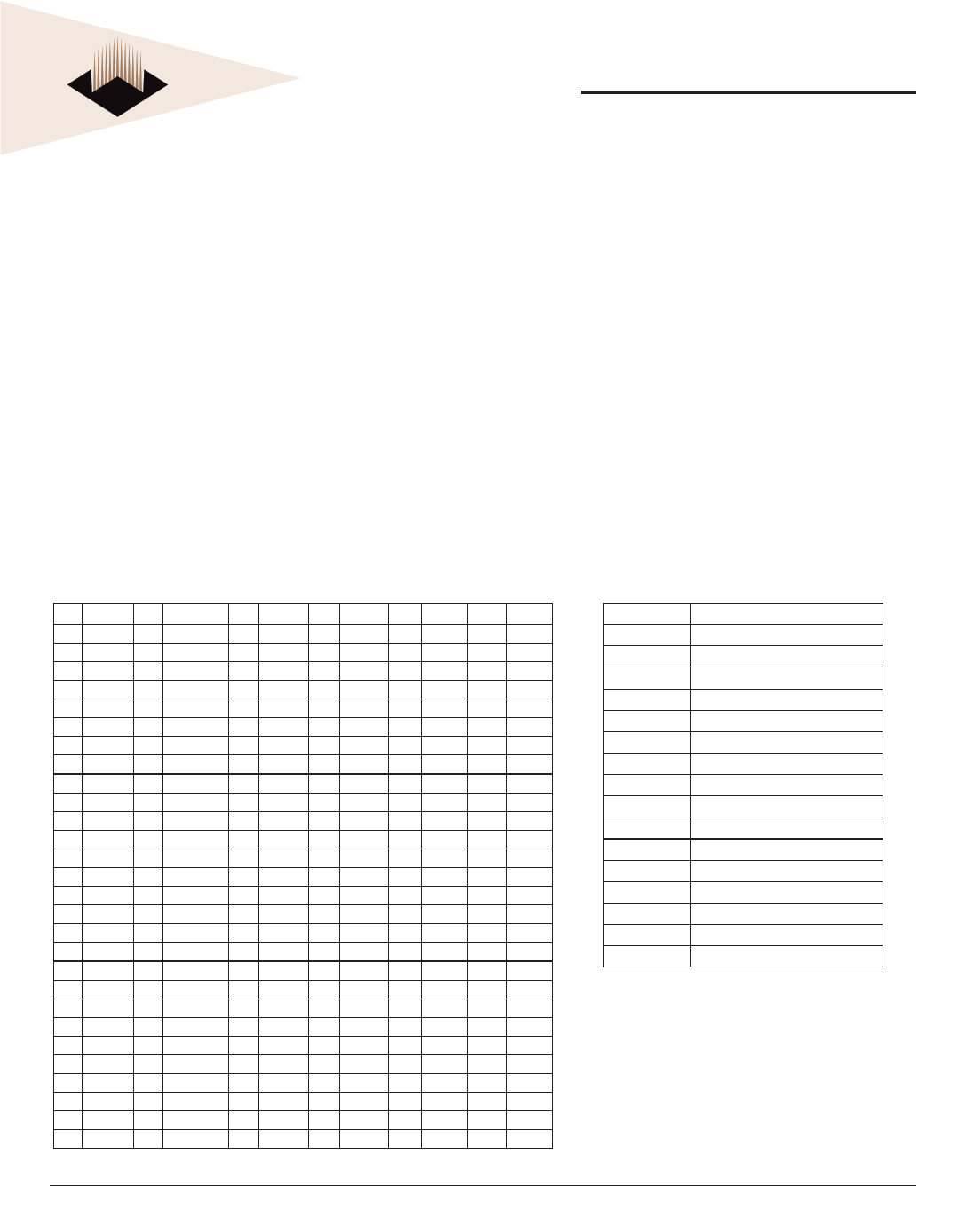
ELECTRICAL CHARACTERISTICS AND RECOMMENDED AC OPERATING CONDITIONS
VCC, VCCQ = +3.3V ±0.3V
AC CHARACTERISTICS
7 7.5 10
PARAMETER
SYMBOL MIN MAX MIN MAX MIN MAX UNITS NOTE
Access timefrom CLK (pos.edge)
CL = 3
tAC(3)
5.4
5.4
6
CL = 2
tAC(2)
5.4
6
6
Address hold time
tAH 0.8
0.8
1
Address setup time
tAS 1.5
1.5
2
CLK high-level width
tCH 2.5
2.5
3
CLK low-level width
tCL 2.5
2.5
3
Clock cycle time
CL = 3
tCK(3)
7
7.5
8
CL = 2
tCK(2)
7.5
10
10
CKE hold time
tCKH 0.8
0.8
1
CKE setup time
tCKS 1.5
1.5
2
www.DCaS#t,aRSASh#e, CeAtS4#,UW.Ec#o, DmQM hold time
tCMH 0.8
0.8
1
CS#, RAS#, CAS#, WE#, DQM setup time
tCMS 1.5
1.5
2
Data-in hold time
tDH 0.8
0.8
1
Data-in setup time
tDS 1.5
1.5
2
Data-out high-impedance time
CL = 3
tHZ(3)
5.4
5.4
6
CL = 2
tHZ(2)
5.4
6
6
Data-out low-impedance time
tLZ 1 1 1
Data-out hold time (load)
tOH 2.7 2.7 2.7
Data-out hold time (no load)
tOHN 1.8 1.8 1.8
ACTIVE to PRECHARGE command
tRAS 37 120,000 44 120,000 50 120,000
ACTIVE to ACTIVE command period
tRC 60
66
66
ACTIVE to READ or WRITE delay
tRCD 15
20
20
Refresh period
tREF 64 64 64
AUTOREFRESH period
tRFC 66 66 66
PRECHARGE command period tRP 15 20 20
ACTIVE bank a to ACTIVE bank b command tRRD 14 15 15
Transition time
tT 0.3 1.2 0.3 1.2 0.3 1.2
WRITE recovery time
tWR 1 CLK
+
7ns
1 CLK
+
7.5ns
1 CLK
+
7.5ns
ns
ns
ns
ns
ns
ns
ns
ns
ns
ns
ns
ns
ns
ns
ns
ns
ns
ns
ns
ns
ns
ns
ms
ns
ns
ns
ns
27
23
23
10
10
28
7
24
14 15 15 ns 25
Exit SELF REFRESH to ACTIVE command
tXSR 67
75
80
ns 20
White Electronic Designs Corp. reserves the right to change products or specifications without notice.
January 2005
Rev. 1
5 White Electronic Designs Corporation • (602) 437-1520 • www.wedc.com
5 Page | ||
| Páginas | Total 9 Páginas | |
| PDF Descargar | [ Datasheet W3DG64126V-D2.PDF ] | |
Hoja de datos destacado
| Número de pieza | Descripción | Fabricantes |
| W3DG64126V-D2 | SDRAM UNBUFFERED | White Electronic Designs |
| Número de pieza | Descripción | Fabricantes |
| SLA6805M | High Voltage 3 phase Motor Driver IC. |
Sanken |
| SDC1742 | 12- and 14-Bit Hybrid Synchro / Resolver-to-Digital Converters. |
Analog Devices |
|
DataSheet.es es una pagina web que funciona como un repositorio de manuales o hoja de datos de muchos de los productos más populares, |
| DataSheet.es | 2020 | Privacy Policy | Contacto | Buscar |