|
|
|
PDF MC33998 Data sheet ( Hoja de datos )
| Número de pieza | MC33998 | |
| Descripción | Switching Power Supply | |
| Fabricantes | Freescale Semiconductor | |
| Logotipo | ||
Hay una vista previa y un enlace de descarga de MC33998 (archivo pdf) en la parte inferior de esta página. Total 20 Páginas | ||
|
No Preview Available !
Freescale Semiconductor
Technical Data
Document Number: MC33998
Rev. 2.0, 8/2006
Switching Power Supply with
Linear Regulators
33998
The 33998 is a medium-power, multi-output power supply
integrated circuit that is capable of operating over a wide input
voltage range, from 6.0 V up to 26.5 V with 40 V transient capability.
It incorporates a sensorless current mode control step-down
switching controller regulating directly to 5.0 V. The 2.6 V linear
regulator uses an external pass transistor to reduce the 33998 power
dissipation. The 33998 also provides a 2.6 V linear standby regulator
and two 5.0 V sensor supply outputs protected by internal low-
resistance LDMOS transistors.
There are two separate enable pins for the main and sensor supply
www.DataSheeto4uUtp.cuotms and standard supervisory functions such as resets with
power-up reset delay.
The 33998 provides proper power supply sequencing for
advanced microprocessor architectures such as the MPC5xx and
683xx microprocessor families.
SWITCHING REGULATOR
DW SUFFIX
EG SUFFIX (PB-FREE)
98ASB42344B
24-PIN SOICW
Features
ORDERING INFORMATION
• Operating Voltage Range 6.0 V up to 26.5 V (40 V transient)
• Step-Down Switching Regulator Output VDDH = 5.0 V @
1400 mA (total)
• Linear Regulator with External Pass Transistor VDDL = 2.6 V @
400 mA
Device
MC33998DW/R2
MCZ33998EG/R2
Temperature
Range (TA)
-40°C to 125°C
Package
24 SOICW
• Low-Power Standby Linear Regulator VKAM = 2.6 V @ 10 mA
• Two 5.0 V @ 200 mA (typical) Sensor Supplies VREF Protected
Against Short-to-Battery and Short-to-Ground with Retry Capability
• Undervoltage Shutdown on the VDDL, VDDH Outputs with Retry Capability
• Reset Signals
• Power-Up Delay
• Enable Pins for Main Supplies (EN) and Sensor Supplies (SNSEN)
• Power Sequencing for Advanced Microprocessor Architectures
• Pb-Free Packaging Designated by Suffix Code EG
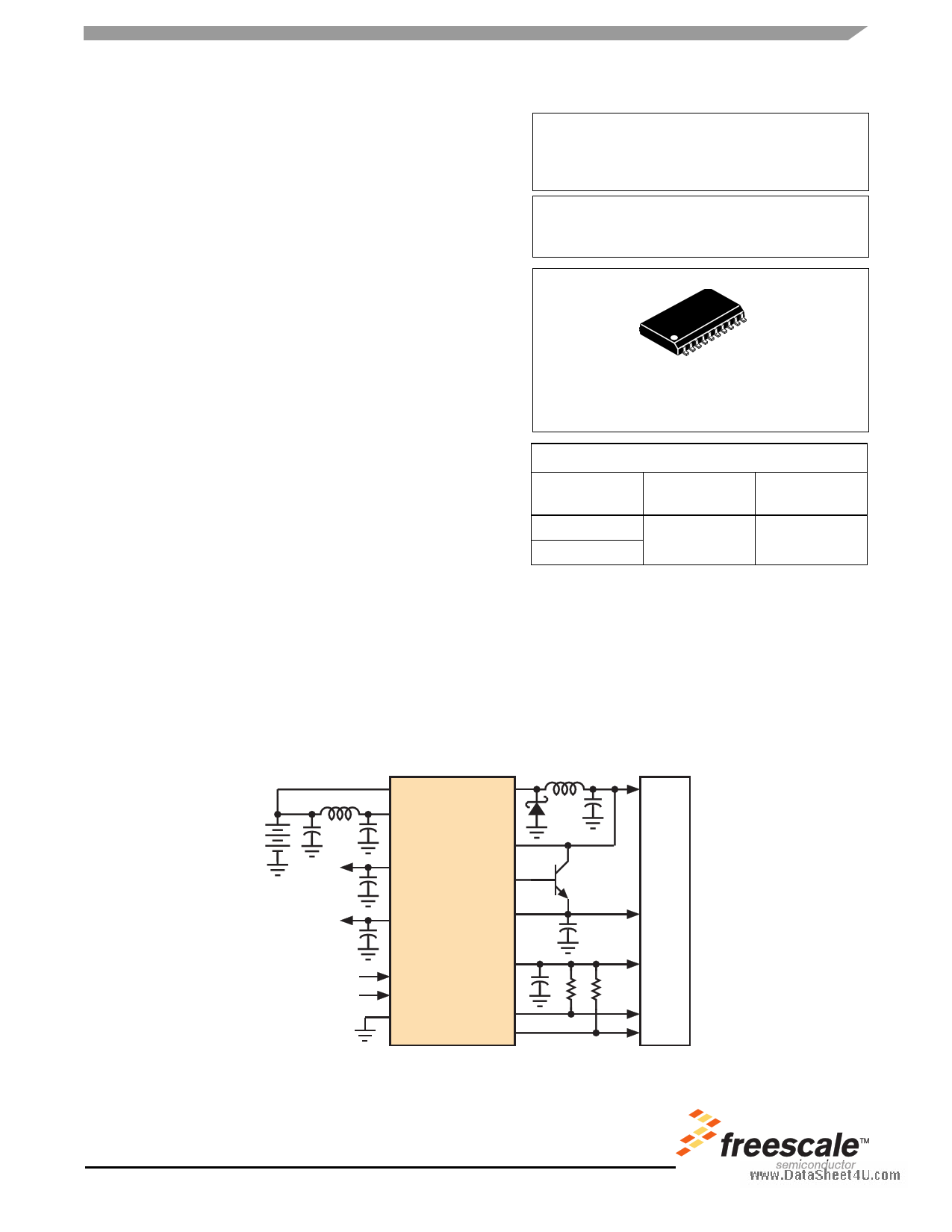
33998
KA_VPWR
VSW
VPWR
VDDH
5.0 V
VDDH
5.0 V VREF1
DRVL
5.0 V VREF2
FBL
EN
SNSEN
GND
VKAM
PWROK
VKAMOK
MCU
VDDL
2.6 V
VKAM
2.6 V
Figure 1. 33998 Simplified Application Diagram
Freescale Semiconductor, Inc. reserves the right to change the detail specifications, as
may be required, to permit improvements in the design of its products.
© Freescale Semiconductor, Inc., 2007. All rights reserved.
1 page 
ELECTRICAL CHARACTERISTICS
MAXIMUM RATINGS
ELECTRICAL CHARACTERISTICS
MAXIMUM RATINGS
Table 2. Maximum Ratings
All voltages are with respect to ground unless otherwise noted.
Rating
Symbol
Value
Unit
Main Supply Voltage
Keep-Alive Supply Voltage
Switching Node
5.0 V Input Power
www.DataSheet4SUe.ncosomr Supply
Keep-Alive Supply Voltage
Maximum Voltage at Logic I/O Pins
VPWR
KA_VPWR
VSW
VDDH
VREF1
VREF2
VKAM
EN
SNSEN
PWROK
VKAMOK
-0.3 to 45
-0.3 to 45
-0.5 to 45
-0.3 to 6.0
-0.3 to 18
-0.3 to 18
-0.3 to 6.0
-0.3 to 6.0
-0.3 to 6.0
-0.3 to 6.0
-0.3 to 6.0
V
V
V
V
V
V
V
Charge Pump Reservoir Capacitor Voltage
Error Amplifier Summing Node
Switching Regulator Output Feedback
CRES
VSUM
FBKB
-0.3 to 18
-0.3 to 6.0
-0.3 to 6.0
V
V
V
VDDL Base Drive
DRVL
-0.3 to 6.0
V
VDDL Feedback
FBL
-0.3 to 6.0
V
ESD Voltage
Human Body Model (all pins) (1)
Machine Model (all pins) (1)
VESD1
VESD2
±500
±100
V
Power Dissipation (TA = 25°C) (2)
Thermal Resistance, Junction to Ambient (3), (4)
Thermal Resistance, Junction to Board (5)
Operational Package Temperature [Ambient Temperature] (6)
PD
RθJA
RθJB
TA
800
60
20
-40 to 125
mW
°C/W
°C/W
°C
Notes
1. ESD1 testing is performed in accordance with the Human Body Model (CZAP=100 pF, RZAP=1500 Ω). ESD2 testing is performed in
accordance with the Machine Model (CZAP=200 pF, RZAP=0 Ω)
2. Maximum power dissipation at indicated junction temperature.
3. Junction temperature is a function of on-chip power dissipation, package thermal resistance, mounting site (board) temperature,
ambient temperature, air flow, power dissipation of other components on the board, and board thermal resistance.
4. Per SEMI G38-87 and JEDEC JESD51-2 with the single layer board horizontal.
5. Thermal resistance between the die and the printed circuit board per JEDEC JESD51-8. Board temperature is measured on the top
surface of the board near the package.
6. The limiting factor is junction temperature, taking into account the power dissipation, thermal resistance, and heat sinking.
33998
5
Analog Integrated Circuit Device Data
Freescale Semiconductor
5 Page 
ELECTRICAL CHARACTERISTICS
DYNAMIC ELECTRICAL CHARACTERISTICS
DYNAMIC ELECTRICAL CHARACTERISTICS
Table 4. DYNAMIC ELECTRICAL CHARACTERISTICS
Characteristics noted under conditions 9.0 V ≤ VPWR ≤ 16 V, -40°C ≤ TJ = TA ≤ 125°C using the typical application circuit (see
Figure 8) unless otherwise noted. Typical values noted reflect the approximate parameter mean at TA = 25°C under nominal
conditions unless otherwise noted.
Characteristic
Symbol
Min
Typ
Max Unit
BUCK REGULATOR (VDDH)
Switching Frequency (14)
Soft Start Duration (see Figure 2)
VPWR = KA_VPWR = 6.0 V
www.DataSheeCt4HUA.cRoGmE PUMP (CRES)
Charge Pump Current Ramp-Up Time
VPWR = KA_VPWR = 14 V, CRES = 22 nF, VCP = 1.0 V to 11 V
Charge Pump Ramp-Up Time
VPWR = KA_VPWR = 7.0 V, CRES = 22 nF, VCP = 7.0 V to 10 V
fSW
tSS
tCRES
tCRES
– 750 – kHz
5.0 –
ms
15
1.0 –
1.0 –
ms
20
ms
10
SENSOR SUPPLIES (VREF1, VREF2)
VREF Overcurrent Detection Time (see Figure 3)
tDET
µs
VREF Load RL = 5.0 Ω to GND, VDDH = 5.1 V, VPWR = KA_VPWR = 10 V,
EN = 5.0 V, SNSEN = 5.0 V
0.5 – 2.0
VREF Retry Timer Delay (see Figure 3)
VREF Load RL = 5.0 Ω to GND, VDDH = 5.1 V, VPWR = KA_VPWR = 10 V,
EN = 5.0 V, SNSEN = 5.0 V
tRET
5.0 –
ms
20
SUPERVISORY CIRCUITS (VPWR)
PWROK Delay Time (Power-On Reset) (see Figure 4)
VKAMOK Delay Time (see Figure 5)
VDDH Power-Up Delay Time (see Figure 6)
Fault-Off Timer Delay Time (see Figure 7)
Notes
14. Guaranteed by design but not production tested.
tD(PWROK)
tD(VKAMOK)
tD(VPWR)
tFAULT
5.0
10
1.0
1.0
–
–
–
–
15 ms
30 ms
10 ms
10 ms
33998
11
Analog Integrated Circuit Device Data
Freescale Semiconductor
11 Page | ||
| Páginas | Total 20 Páginas | |
| PDF Descargar | [ Datasheet MC33998.PDF ] | |
Hoja de datos destacado
| Número de pieza | Descripción | Fabricantes |
| MC3399 | AUTOMOTIVE HALF-AMP HIGH-SIDE SWITCH | Motorola Semiconductors |
| MC33990 | Enhanced Class B Serial Transceiver | Freescale Semiconductor |
| MC33991 | Gauge Driver Integrated Circuit | Motorola Semiconductors |
| MC33993 | Multiple Switch Detection Interface | Motorola Semiconductors |
| Número de pieza | Descripción | Fabricantes |
| SLA6805M | High Voltage 3 phase Motor Driver IC. |
Sanken |
| SDC1742 | 12- and 14-Bit Hybrid Synchro / Resolver-to-Digital Converters. |
Analog Devices |
|
DataSheet.es es una pagina web que funciona como un repositorio de manuales o hoja de datos de muchos de los productos más populares, |
| DataSheet.es | 2020 | Privacy Policy | Contacto | Buscar |