|
|
|
PDF ON1120 Data sheet ( Hoja de datos )
| Número de pieza | ON1120 | |
| Descripción | Transmissive Photosensors | |
| Fabricantes | Panasonic Semiconductor | |
| Logotipo | ||
Hay una vista previa y un enlace de descarga de ON1120 (archivo pdf) en la parte inferior de esta página. Total 2 Páginas | ||
|
No Preview Available !
Transmissive Photosensors (Photo lnterrupters)
CNZ1120 (ON1120)
Photo lnterrupter
For contactless SW, object detection
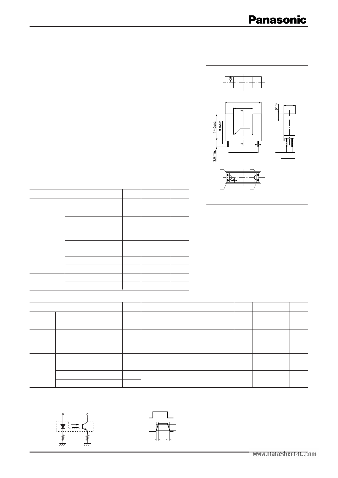
Unit: mm
■ Overview
CNZ1120 is a photocoupler in which a high efficiency GaAs
infrared light emitting diode is used as the light emitting element,
and a high sensitivity phototransistor is used as the light detecting
element. The two elements are arranged so as to face each other,
and objects passing between them are detected.
19.0±0.35
10.0±0.3
A
6.2±0.25
■ Features
• Wide gap between emitting and detecting elements, suitable for
thick plate detection
Gap: 10 mm
www.DataShe•eFt4aUst.creosmponse: tr , tf = 6 µs (typ.)
• The external case is molded using visible light cutoff resin. The case
has no openings, so the photosensor is not easily susceptible to
output attenuation resulting from dust or particles
■ Absolute Maximum Ratings Ta = 25°C
Parameter
Symbol Rating
Input (Light Reverse voltage
emitting diode) Forward current
Power dissipation *1
Output (Photo Collector-emitter voltage
transistor) (Base open)
VR
IF
PD
VCEO
3
50
75
20
Unit
V
mA
mW
V
2-C0.5
A'
(15.5)
2-0.45
(2.54)
SEC. A-A'
23
1: Anode
2: Cathode
3: Collector
1 4 4: Emitter
PISTR104-014 Package
(Note) ( ) Dimension is reference
Emitter-collector voltage VECO
(Base open)
5
V
Temperature
Collector current
Collector power dissipation *2
Operating ambient temperature
Storage temperature
IC
PC
Topr
Tstg
20
100
−5 to +60
−15 to +65
mA
mW
°C
°C
■ Electrical-Optical Characteristics Ta = 25°C ± 3°C
Note) *1: Input power derating ratio is 1.88 mW/°C at
Ta ≥ 25°C.
*2: Output power derating ratio is 2.50 mW/°C
at Ta ≥ 25°C.
Parameter
Symbol
Conditions
Min Typ Max Unit
Input Forward voltage
VF
characteristics Reverse current
IR
Output
Collector-emitter cutoff current ICEO
characteristics (Base open)
Collector-emitter capacitance CC
Transfer Collector current
IC
characteristics Collector-emitter saturation voltage VCE(sat)
Rise time *
Fall time *
tr
tf
IF = 50 mA
VR = 3 V
VCE = 10 V, IF = 0 mA, ID = 0 mA
VCE = 10 V, f = 1 MHz
VCE = 10 V, IF = 20 mA, RL = 100 Ω
IF = 50 mA, IC = 0.1 mA
VCC = 10 V, IC = 1 mA, RL = 100 Ω
1.2 1.5 V
10 µA
200 nA
5 pF
1.0 mA
0.4 V
6 µs
6 µs
Note) 1. Input and output are practiced by electricity.
2. This device is designed be disregarded radiation.
3. *: Switching time measurement circuit
Sig. in
50Ω
VCC
Sig. out
RL
(Input pulse)
(Output pulse)
tr : Rise time
90% tf : Fall time
10%
tr tf
Note) The part number in the parenthesis shows conventional part number.
Publication date: April 2004
SHG00032BED
1
1 page | ||
| Páginas | Total 2 Páginas | |
| PDF Descargar | [ Datasheet ON1120.PDF ] | |
Hoja de datos destacado
| Número de pieza | Descripción | Fabricantes |
| ON1120 | Transmissive Photosensors | Panasonic Semiconductor |
| Número de pieza | Descripción | Fabricantes |
| SLA6805M | High Voltage 3 phase Motor Driver IC. |
Sanken |
| SDC1742 | 12- and 14-Bit Hybrid Synchro / Resolver-to-Digital Converters. |
Analog Devices |
|
DataSheet.es es una pagina web que funciona como un repositorio de manuales o hoja de datos de muchos de los productos más populares, |
| DataSheet.es | 2020 | Privacy Policy | Contacto | Buscar |