|
|
|
PDF R8A66120FFA Data sheet ( Hoja de datos )
| Número de pieza | R8A66120FFA | |
| Descripción | 4M-bit x 2 MULTIPLE FIELD MEMORY | |
| Fabricantes | Renesas Technology | |
| Logotipo | ||
Hay una vista previa y un enlace de descarga de R8A66120FFA (archivo pdf) en la parte inferior de esta página. Total 15 Páginas | ||
|
No Preview Available !
R8A66120FFA
4M-bit x 2 MULTIPLE FIELD MEMORY
RJJ03FXXXREJ03F0161-0170
Rev.1.70
May.16.2008
Description
R8A66120FFA is high-speed field memory with two FIFO (First In First Out) memories of
4M-bit, which uses high-performance silicon gate process technology.
Features
•Total memory Capacity
8Mega-bit
•High speed operation
cycle time
10.0ns(Min.)
output access time 6.0ns(Max.)
•Output hold time
•Supply voltage
1.0ns(Min.)
3.3 ± 0.3V
fmax = 100MHz
www.DataSheet4U.com
•Variable length delay bit
•Synchronous write/read operation
•3 states output
•Package
PLQP0048KB-A (48P6Q-A)
( 48pins 7x7mm body LQFP )
Application
W-CDMA base station, Digital PPC, Digital TV,VTR and so on.
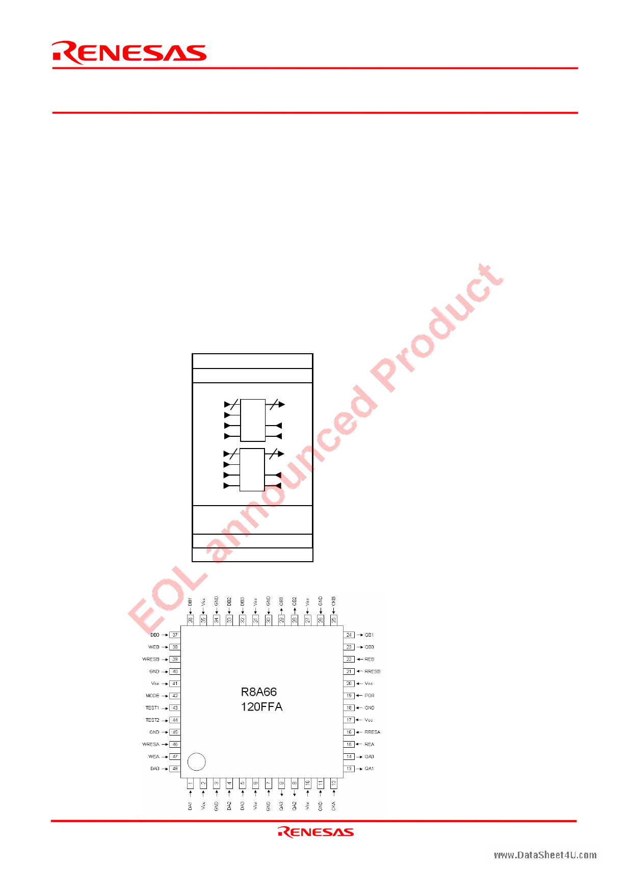
Mode Descriptions
1K-word = 1024-words
1024K-word
4bit bus I/F
4
DA<3:0>
CKA
WRESA
WEA
4
1024K-w
X
4-bit
FIFO
4
DB<3:0>
CKB
WRESB
WEB
4
1024K-w
X
4-bit
FIFO
QA<3:0>
RRESA
REA
QB<3:0>
RRESB
REB
The 2 pieces of 1024K-word x 4-bit
FIFO can be operated completely
independently.
2-system individual input
2-system individual output
Pin Configuration (Top view)
REJ03F0161-0170 Rev.1.70 May.16.2008
page 1 of 14
Outline: PLQP0048KB-A (48P6Q-A)
1 page 
R8A66120FFA
Power On
After power-on this IC, some circuits of internal FIFO should be initialized by the following procedures (1), (2).
Also, when the supply voltage (Vcc) drops below the operation voltage range(3.0 to 3.6V) during operating and so this is powered
on again, they should be initialized by the same procedures.
(1)After 1msec or more has passed under the following conditions (i), (ii) and (iii), please input the signal of “L” to “H” to POR pin
for power on reset. After of that, POR pin should be fixed at "H".
(i) :Vcc reaches to the operation voltage range.
(ii) :The clock signal is inputted to CK pin
(iii) :POR pin is fixed at "L".
(2)After POR pin is fixed at “H”, write reset and read reset operations should be provided with 100 cycles or more respectively.
There is no problem in these reset operations, if total reset cycles reach to 100 or more even if those are discontinuous.
www.DataSheet4U.com
Pin nam e 3.0V~3.6V
Vcc
GND
CK
GND
POR
GND
WRES
RRES
Vcc
Vcc
1msec or more
100 cycles or more of continuous or
discontinuous reset operation
GND
Vcc
Vcc
REJ03F0161-0170 Rev.1.70 May.16.2008
page 5 of 14
5 Page 
R8A66120FFA
Variable Length Delay bits
The 1-line length (cycle number) of R8A66120FFA is 1,048,576-cycle.
1-line Delay
In read cycles, an output data is read out at the (first) rising edge of CK (i.e. the start of the cycle ) .
In write cycles, an input data is written at the (second) rising edge of CK (i.e. the end of the cycle ) .
So 1-line delay can be made easily according to the control method of the following figure.
www.DataSheet4U.com
CK
Reset
cycle
0 cycle
1 cycle
2 cycle
1048574
cycle
1048575
cycle
1048576 (0’)
cycle
0 cycle
1048577 (1’)
cycle
1048578 (2’)
cycle
・・・Write
side
1 cycle
2 cycle ・・・Read side
WRES
RRES
Dn
Qn
(0)
(1)
(2)
(1048573)
(1048574)
(1048575)
(0’)
(1’)
(2’)
1048576 cycle
(0) (1)
WE, RE=“L”
(2)
N-bit Delay 1
(Reset at cycles corresponding to delay length)
Reset cycle 0 cycle
1 cycle
2 cycle
CK
n-1 cycle
Reset cycle
0’ cycle
0 cycle
1’ cycle
1 cycle
2’ cycle
2 cycle
・・・Write side
・・・Read side
WRES
RRES
Dn
(0) (1)
(2)
(n-2)
(n-1)
(0’) (1’) (2’)
Delay length n
Qn (0) (1)
1048576 in 256
WE, RE=“L”
Note: Take care of the restriction to a interval between a write cycle and a read cycle (ref. page10).
REJ03F0161-0170 Rev.1.70 May.16.2008
page 11 of 14
(2)
11 Page | ||
| Páginas | Total 15 Páginas | |
| PDF Descargar | [ Datasheet R8A66120FFA.PDF ] | |
Hoja de datos destacado
| Número de pieza | Descripción | Fabricantes |
| R8A66120FFA | 4M-bit x 2 MULTIPLE FIELD MEMORY | Renesas Technology |
| Número de pieza | Descripción | Fabricantes |
| SLA6805M | High Voltage 3 phase Motor Driver IC. |
Sanken |
| SDC1742 | 12- and 14-Bit Hybrid Synchro / Resolver-to-Digital Converters. |
Analog Devices |
|
DataSheet.es es una pagina web que funciona como un repositorio de manuales o hoja de datos de muchos de los productos más populares, |
| DataSheet.es | 2020 | Privacy Policy | Contacto | Buscar |