|
|
|
PDF ST2S06D33 Data sheet ( Hoja de datos )
| Número de pieza | ST2S06D33 | |
| Descripción | (ST2S06xxx) Dual synchronous rectification | |
| Fabricantes | STMicroelectronics | |
| Logotipo | ||
Hay una vista previa y un enlace de descarga de ST2S06D33 (archivo pdf) en la parte inferior de esta página. Total 21 Páginas | ||
|
No Preview Available !
ST2S06A33
ST2S06B - ST2S06D33
Dual synchronous rectification with reset or inhibit, 0.5 A, 1.5 MHz
adjustable step-down switching regulator
Features
■ Step-down current mode PWM (1.5 MHz)
DC-DC converter
■ Fixed or adjustable output voltage from 0.8 V
www.DataSheet4U.com
■ 2% DC output voltage tolerance
■ Synchronous rectification
■ Reset function for A and D versions
■ Inhibit function for B version
■ Internal soft start for start-up current limitation
and power ON delay of 50-100 µs
■ Typical efficiency: > 90%
■ 0.5 A output current capability
■ Non-switching quiescent current: max 1 mA
over temperature range
■ RDS(ON) 150 mΩ (typ.)
■ Uses tiny capacitors and inductors
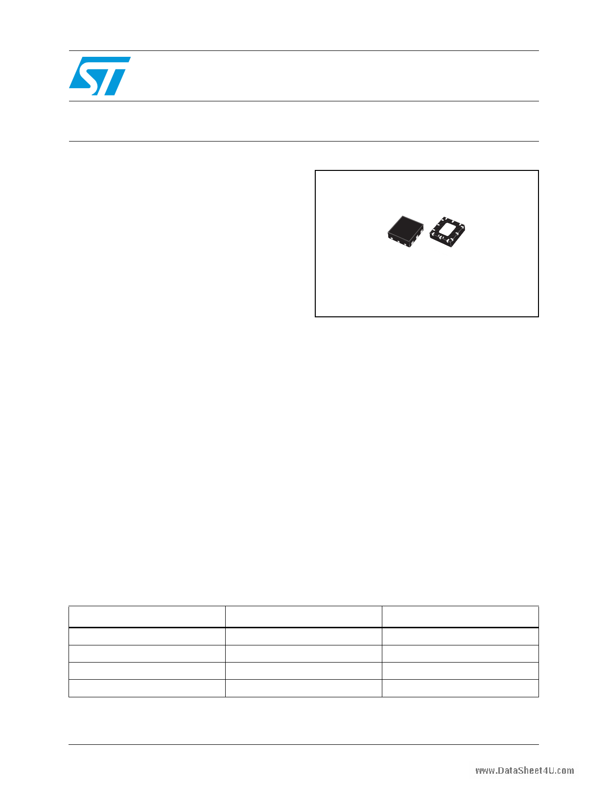
■ Available in QFN12L (4x4 mm)
Description
The ST2S06 is a dual step-down DC-DC
converter optimized for powering low-voltage
digital cores in ODD applications and, generally,
to replace the high current linear solution when
QFN12L (4x4 mm)
the power dissipation may cause a high heating of
the application environment. It provides up to 0.5
A over an input voltage range of 2.5 V to 5.5 V.
A high switching frequency of 1.5 MHz allows the
use of tiny surface-mount components as well as
a resistor divider to set the output voltage value.
Only an inductor and two capacitors are required.
A low output ripple is guaranteed by the current
mode PWM topology and the utilization of low
ESR SMD ceramic capacitors. The device is
thermally protected and current limited to prevent
damage due to accidental short circuit. The
ST2S06 series is available in the QFN12L (4x4
mm) package.
Table 1. Device summary
Order code
ST2S06APQR(1)
ST2S06A33PQR
ST2S06D33PQR
ST2S06BPQR
1. Available on request.
March 2008
Package
QFN12L (4x4 mm)
QFN12L (4x4 mm)
QFN12L (4x4 mm)
QFN12L (4x4 mm)
Rev 3
Packaging
Tape and reel
Tape and reel
Tape and reel
Tape and reel
1/21
www.st.com
21
1 page 
ST2S06A33 - ST2S06B - ST2S06D33
3 Maximum ratings
Maximum ratings
Table 3. Absolute maximum ratings
Symbol
Parameter
VIN_SW
VIN_A
VINH
SWITCH voltage
Positive power supply voltage
Positive power supply voltage
Inhibit voltage
Max. voltage of output pin
VFB1,2/VO1
www.DataSheet4U.com VO1
Current into VFB
pin
Feedback voltage/output voltage
Output voltage (for VO > 1.6 V)
Common mode input voltage
TJ
TSTG
TLEAD
Max junction temperature
Storage temperature range
Lead temperature (soldering) 10 sec.
Value
-0.3 to 7
-0.3 to 7
-0.3 to 7
-0.3 to 7
-0.3 to 2.5
-0.3 to 5
+1 to -1
150
-65 to +150
300
Unit
V
V
V
V
V
V
mA
°C
°C
°C
Note:
Absolute maximum ratings are those values beyond which damage to the device may occur.
Functional operation under these conditions is not implied.
Table 4. Thermal data
Symbol
Parameter
RthJC
RthJA
Thermal resistance junction-case
Thermal resistance junction-ambient
Value
10
60
Unit
°C/W
°C/W
Table 5. ESD performance
Symbol
Parameter
ESD ESD protection voltage
Test conditions
HBM-DH11C
Value
4
Unit
kV
5/21
5 Page 
ST2S06A33 - ST2S06B - ST2S06D33
Typical performance characteristics
Figure 9. Switching frequency vs.
temperature (ST2S06B)
Figure 10. Inhibit threshold vs. temperature
(ST2S06B)
1.9
1.8
1.7
1.6
1.5
1.4
1.3
1.2
1.1
www.DataSheet4U.com -50
-25
0 25 50 75
Temperature [°C]
100 125
1.4
VI=5V, IO1= IO2=100mA
1.2 ON
1
0.8
OFF
0.6
0.4
0.2
0
-50 -25 0 25 50 75 100 125
T [C°]
Figure 11. Switching current limitation vs.
input voltage (ST2S06A)
Figure 12. PMOS switch on resistance vs.
temperature
2
VI from 2.5V to 5.5V, Output2 Maximum load Current
1.8
1.6
240
220
200
180
VCC=5V, ISW=250mA
1.4 160
140
1.2
120
1 100
2.5 3 3.5 4 4.5 5 5.5
-50 -25 0 25 50 75 100 125
VI [V]
T [°C]
Figure 13. NMOS switch on resistance vs.
temperature
Figure 14. Delay time vs. temperature
(ST2S06A)
170
150
130
110
90
70
VCC=5V, ISW=250mA
VI
VRES
50
-50 -25 0 25 50 75 100 125
T [°C]
VI Rising from 0V to 5V, Delay from VRES threshold and
reset pin below 0V.
11/21
11 Page | ||
| Páginas | Total 21 Páginas | |
| PDF Descargar | [ Datasheet ST2S06D33.PDF ] | |
Hoja de datos destacado
| Número de pieza | Descripción | Fabricantes |
| ST2S06D33 | (ST2S06xxx) Dual synchronous rectification | STMicroelectronics |
| Número de pieza | Descripción | Fabricantes |
| SLA6805M | High Voltage 3 phase Motor Driver IC. |
Sanken |
| SDC1742 | 12- and 14-Bit Hybrid Synchro / Resolver-to-Digital Converters. |
Analog Devices |
|
DataSheet.es es una pagina web que funciona como un repositorio de manuales o hoja de datos de muchos de los productos más populares, |
| DataSheet.es | 2020 | Privacy Policy | Contacto | Buscar |