|
|
PDF SPWNE555D Data sheet ( Hoja de datos )
| Número de pieza | SPWNE555D | |
| Descripción | Single Timer | |
| Fabricantes | SeCoS | |
| Logotipo |  |
|
Hay una vista previa y un enlace de descarga de SPWNE555D (archivo pdf) en la parte inferior de esta página. Total 5 Páginas | ||
|
No Preview Available !
Elektronische Bauelemente
SPWNE555D
Single Timer
www.datasheet4u.com
Description
RoHS Compliant Product
The SPWNE555D is a highly stable timer integrated circuit. It
can be operated in Astable mode and Monostable mode. With
monostable operation, the time delay is controlled by one
external and one capacitor. With a stable operation, the frequency
and duty cycle are accurately controlled with two external resistors
and one capacitor.
DIP-8
D
GAUGE PLANE
Features
* Turn Off Time Less Than 2uSec
* Adjustable Duty Cycle
* Timing From uSec to Hours
* High Current Driver Capability (=200mA)
Applications
* Time Delay Generation
* Pulse Generation
* Precistion Timing
SEATING PLANE
ZZ
be
b
SECTION Z - Z
REF.
A
A1
A2
b
b1
b2
b3
c
Millimeter
Min. Max.
- 0.5334
0.381
-
2.921
4.953
0.356
0.559
0.356
0.508
1.143
1.778
0.762
1.143
0.203
0.356
REF.
c1
D
E
E1
e
HE
L
Millimeter
Min. Max.
0.203
0.279
9.017
10.16
6.096
7.112
7.620
8.255
2.540 BSC
- 10.92
2.921
3.810
Block Diagram & Pin Configuration
rogrammed by
pacitor CT to ground .Operation 500kHz
nts up to
This is the reference output .It provides charging current for capacitor CT
http://www.SeCoSGmbH.com/
01-Jun-2002 Rev. A
Any changing of specification will not be informed individual
Page 1 of 5
1 page 
Elektronische Bauelemente
www.dAaptasphleiect4aut.cioomn Circuit
SPWNE555D
Single Timer
FLIP-FLOP
Application Notes
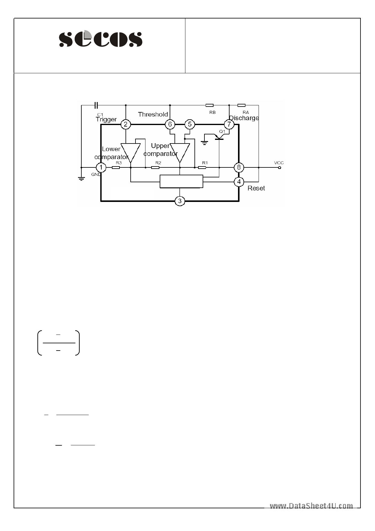
The application circuit shows astable mode configuration.
Pin 6 (Threshold) is tied to Pin 2 (Trigger) and Pin 4 (Reset) is tied to VCC (Pin 8). The external capacitor C1
of Pin 6 and Pin 2 charges through RA, RB and discharge through RB only. In the internal circuit of SPWNE555D,
one input of the upper comparator is at voltage of 2/3VCC (R1=R2=R3), another input is connected to Pin 6. As
soon as C1 is charging to higher than 2/3VCC, transistor Q1 is turned ON and discharge C1 to collector voltage
of transistor Q1. Therefore, the flip-flop circuit is reset and output is low. One input of lower comparator is at
voltage of 1/3VCC, discharge transistor Q1 turn off and C1 charges through RA and RB. Therefore, flip-flop
circuit is set output high.
That is, when C1 charges through RA and RB, output is high and when C1 discharge through RB, output is
low. The charge time (output is high) t1 is 0.693 (RA+RB) C1 and the discharge time (output is low) T2 is
0.693RB*C1.
VVcccc-
1
3
VVcccc
In
VVcccc-
2
13
VVVcccccc
=0.693
Thus the total period time T is given by
T1=0.693*(RA+RB)*C1
T2=0.693*RB*C1
T=T1+T2=0.693(RA+2RB)*C1.
Then the frequency of astable mode is given by
1 11..4444
f = T = ((RRAA++22RRBB))**CC11
The duty cycle is given by
T2 RB
D.C. = T = RRAA++22RRBB .
http://www.SeCoSGmbH.com/
01-Jun-2002 Rev. A
Any changing of specification will not be informed individual
Page 5 of 5
5 Page | ||
| Páginas | Total 5 Páginas | |
| PDF Descargar | [ Datasheet SPWNE555D.PDF ] | |
Hoja de datos destacado
| Número de pieza | Descripción | Fabricantes |
| SPWNE555D | Single Timer | SeCoS |
| Número de pieza | Descripción | Fabricantes |
| SLA6805M | High Voltage 3 phase Motor Driver IC. |
Sanken |
| SDC1742 | 12- and 14-Bit Hybrid Synchro / Resolver-to-Digital Converters. |
Analog Devices |
|
DataSheet.es es una pagina web que funciona como un repositorio de manuales o hoja de datos de muchos de los productos más populares, |
| DataSheet.es | 2020 | Privacy Policy | Contacto | Buscar |
