|
|
|
PDF LTC3831-1 Data sheet ( Hoja de datos )
| Número de pieza | LTC3831-1 | |
| Descripción | High Power Synchronous Switching Regulator Controller | |
| Fabricantes | Linear Technology | |
| Logotipo | ||
Hay una vista previa y un enlace de descarga de LTC3831-1 (archivo pdf) en la parte inferior de esta página. Total 20 Páginas | ||
|
No Preview Available !
FEATURESwww.datasheet4u.com
s VOUT as Low as 0.4V
s High Power Switching Regulator Controller
for DDR Memory Termination
s VOUT Tracks 1/2 of VIN or External VREF
s No Current Sense Resistor Required
s Low VCC Supply: 3V to 8V
s Maximum Duty Cycle > 91% Over Temperature
s Drives All N-Channel External MOSFETs
s High Efficiency: Up to 95%
s Programmable Fixed Frequency Operation:
100kHz to 500kHz
s External Clock Synchronization Operation
s Programmable Soft-Start
s Low Shutdown Current: <10µA
s Overtemperature Protection
s Available in 16-PUin Narrow SSOP Package
APPLICATIO S
s DDR SDRAM Termination
s SSTL_2, SSTL_3 Interface
s HSTL Interface
LTC3831-1
High Power Synchronous
Switching Regulator Controller
for DDR Memory Termination
DESCRIPTIO
The LTC®3831-1 is a high power, high efficiency switch-
ing regulator controller designed for DDR memory termi-
nation. The LTC3831-1 generates an output voltage equal
to 1/2 of an external supply or reference voltage. The
LTC3831-1 uses a synchronous switching architecture
with N-channel MOSFETs. Additionally, the chip senses
output current through the drain-source resistance of the
upper N-channel FET, providing an adjustable current
limit without a current sense resistor.
The LTC3831-1 operates with input supply voltage as low
as 3V and with a maximum duty cycle of > 91%. It includes
a fixed frequency PWM oscillator for low output ripple
operation. The 300kHz free-running clock frequency can
be externally adjusted or synchronized with an external
signal from 100kHz to above 500kHz. In shutdown mode,
the LTC3831-1 supply current drops to <10µA.
, LTC and LT are registered trademarks of Linear Technology Corporation.
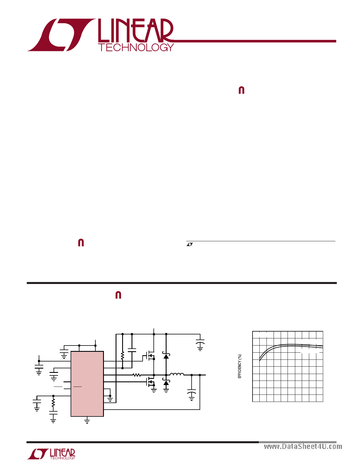
TYPICAL APPLICATIO
0.75V DDR Memory Termination Application
VDDQ
1.5V
12V
3.3V 4.7µF
2.2µF
0.01µF
PVCC2
VCC
PVCC1
TG
SS IMAX
LTC3831-1 IFB
FREQSET
BG
SHDN
SHDN
PGND
68pF 1k
COMP
GND
R+
22nF
R– FB
0.1µF
4.7k
1k
+
220µF
1.3µH
+
180µF
VTT
(VOUT)
0.75V
±10A
38311 TA01a
Efficiency vs Load Current
100
TA = 25°C
90
80
70
VDDQ = 1.8V
VDDQ = 1.5V
60
50
40
30
20
10
0
0 1 2 3 4 5 6 7 8 9 10
LOAD CURRENT (A)
3831 TAO1b
38311f
1
1 page 
TYPICAL PERFOR A CE CHARACTERISTICS
Maximum TG Duty Cycle
vs Temperature
www.da10ta0sheet4u.com
VFB = 0V
99 REFER TO FRONT PAGE APPLICATION
98
97
96
95
94
93
92
91
–50 –25
0 25 50 75
TEMPERATURE (°C)
100 125
3831 G11
Output Current Limit Threshold
vs Temperature
15
14
13
12
11
10
9
8
7
6
5
4
3
2
1 REFER TO FRONT PAGE APPLICATION
0
–50 –25 0 25 50 75 100
TEMPERATURE (°C)
125
3831 G14
Undervoltage Lockout Threshold
Voltage vs Temperature
3.0
2.9
2.8
2.7
2.6
2.5
2.4
2.3
2.2
2.1
2.0
–50 –25
0 25 50 75 100 125
TEMPERATURE (°C)
3831 G17
IMAX Sink Current
vs Temperature
20
18
16
14
12
10
8
6
4
– 50 – 25
0 25 50 75
TEMPERATURE (°C)
100 125
3831 G12
Soft-Start Source Current
vs Temperature
–8
–9
–10
–11
–12
–13
–14
–15
–16
– 50 – 25
0 25 50 75
TEMPERATURE (°C)
100 125
3831 G15
VCC Operating Supply Current
vs Temperature
1.6
FREQSET FLOATING
1.5
1.4
1.3
1.2
1.1
1.0
0.9
0.8
0.7
0.6
0.5
0.4
–50 –25
0 25 50 75
TEMPERATURE (°C)
100 125
3831 G18
LTC3831-1
Output Overcurrent Protection
0.8
0.7
0.6
0.5
0.4
0.3
0.2
0.1 TA = 25°C
REFER TO FRONT PAGE APPLICATION
0
0 2 4 6 8 10 12
OUTPUT CURRENT (A)
14
3831 G13
Soft-Start Sink Current
vs (VIFB – VIMAX)
2.00
TA = 25°C
1.75
1.50
1.25
1.00
0.75
0.50
0.25
0
–150 –125 –100 –75 –50
VIFB – VIMAX (mV)
–25 0
3831 G16
PVCC Supply Current
vs Oscillator Frequency
90
TA = 25°C
80
70
60
TG AND BG LOADED
WITH 6800pF,
PVCC1,2 = 12V
50 TG AND BG
40
LOADED
WITH 1000pF,
30 PVCC1,2 = 5V
TG AND BG
LOADED
WITH 6800pF,
PVCC1,2 = 5V
20
10
0
0 100 200 300 400 500
OSCILLATOR FREQUENCY (kHz)
3831 G19
38311f
5
5 Page 
LTC3831-1
APPLICATIO S I FOR ATIO
external clock frequency goes higher. The effect of this
decrease in ramp amplitude increases the open-loop gain
wwwo.dfattahseheecto4un.tcroomller feedback loop. As a result, the loop
crossover frequency increases and it may cause the feed-
back loop to be unstable if the phase margin is insufficient.
To overcome this problem, the LTC3831-1 monitors the
peak voltage of the ramp signal and adjust the oscillator
charging current to maintain a constant ramp peak.
SHDN
200kHz
FREE RUNNING
RAMP SIGNAL
TRADITIONAL
SYNC METHOD
WITH EARLY
RAMP
TERMINATION
RAMP SIGNAL
WITH EXT SYNC
RAMP AMPLITUDE
ADJUSTED
LTC3831
KEEPS RAMP
AMPLITUDE
CONSTANT
UNDER SYNC
38311 F03
Figure 3. External Synchronization Operation
Input Supply Considerations/Charge Pump
The LTC3831-1 requires four supply voltages to operate:
VIN for the main power input, PVCC1 and PVCC2 for MOS-
FET gate drive and a clean, low ripple VCC for the LTC3831-1
internal circuitry (Figure 4). VIN is usually connected to
VDDQ in most DDR memory termination applications.
The VCC supply can be as low as 3V and the quiescent
current is typically 800µA. Place a 4.7µA bypass capacitor
as close as possible to this pin. Gate drive for the top
N-channel MOSFET Q1 is supplied from PVCC1. This
supply must be above VIN by at least one power MOSFET
VGS(ON) for efficient operation. In addition, this supply
must be higher that VCC by at least 2V for normal opera-
tion. An internal level shifter allows PVCC1 to operate at
voltages above VCC and VIN, up to 14V maximum. This
higher voltage can be supplied with a separate supply, or
it can be generated using a charge pump.
Gate drive for the bottom MOSFET Q2 is provided through
PVCC2. This supply only needs to be above the power
MOSFET VGS(ON) for efficient operation. PVCC2 can also be
driven from the same supply/charge pump for the PVCC1,
or it can be connected to a lower supply to improve
efficiency.
In a typical low voltage DDR memory termination applica-
tion, VIN or VDDQ can be a low as 1.5V. If the only available
supply for the LTC3831-1 is 3.3V, a tripling charge pump
circuit can be added to power the PVCC1 and PVCC2 pins.
This requires sub-logic level threshold power MOSFET
with RDS(ON) specified at VGS = 2.5V.
Figure 5 shows a tripling charge pump circuit that powers
the PVCC1 and PVCC2 pins. This circuit provides (VCC +
2VIN – 3VF) to PVCC1 while Q1 is ON and (VCC + VIN – 2VF)
to PVCC2 where VF is the ON voltage of the Schottky diode.
The circuit requires the use of Schottky diodes to minimize
forward drop across the diodes at start-up. The tripling
charge pump circuit will tend to rectify any ringing at the
drain of Q2 and can provide well more than (VCC + 2VIN)
at PVCC1. A 12V zener diode may be included from PVCC1
to PGND to prevent transients from damaging the circuitry
at PVCC1 or the gate of Q1.
VCC PVCC2 PVCC1
VIN
INTERNAL
CIRCUITRY
LTC3831-1
TG
Q1
LO
VOUT
BG
Q2
+
COUT
38311 F04
Figure 4. Input Supplies
38311f
11
11 Page | ||
| Páginas | Total 20 Páginas | |
| PDF Descargar | [ Datasheet LTC3831-1.PDF ] | |
Hoja de datos destacado
| Número de pieza | Descripción | Fabricantes |
| LTC3831-1 | High Power Synchronous Switching Regulator Controller | Linear Technology |
| Número de pieza | Descripción | Fabricantes |
| SLA6805M | High Voltage 3 phase Motor Driver IC. |
Sanken |
| SDC1742 | 12- and 14-Bit Hybrid Synchro / Resolver-to-Digital Converters. |
Analog Devices |
|
DataSheet.es es una pagina web que funciona como un repositorio de manuales o hoja de datos de muchos de los productos más populares, |
| DataSheet.es | 2020 | Privacy Policy | Contacto | Buscar |