|
|
|
PDF MW7IC2750NR1 Data sheet ( Hoja de datos )
| Número de pieza | MW7IC2750NR1 | |
| Descripción | RF Power Field Effect Transistors N-Channel Enhancement-Mode Lateral MOSFETs | |
| Fabricantes | Freescale Semiconductor | |
| Logotipo | ||
Hay una vista previa y un enlace de descarga de MW7IC2750NR1 (archivo pdf) en la parte inferior de esta página. Total 25 Páginas | ||
|
No Preview Available !
Freescale Semiconductor
Technical Data
Document Number: MW7IC2750N
Rev. 0, 5/2008
RF Power Field Effect Transistors
N - Channel Enhancement - Mode Lateral MOSFETs
Designed for WiMAX base station applications with frequencies up to
2700 MHz. Suitable for WiMAX, WiBro, BWA, and OFDM multicarrier Class
www.datasAhBeeat4nud.cComlass C amplifier applications.
• T1P0yopuMtic=Hal8zWCWihMaatAtnsXnAePlvegBr.a,fonfrd=mw2aid7nt0che0,:IMnVpHDuDzt,=S8i02g28n.a1Vl6oPdltA,sR,64ID=QQ91A.5=Md13B6/40@, m4 0Ab.,u0Ir1Ds%tQs2,P=ro5b5a0bmilitAy,
on CCDF.
Power Gain — 26 dB
Power Added Efficiency — 17%
Device Output Signal PAR — 8.6 dB @ 0.01% Probability on CCDF
ACPR @ 8.5 MHz Offset — - 49 dBc in 1 MHz Channel Bandwidth
Driver Applications
•
CTPyohpuatinc=anl4eWlWBiMaatnAtsdXwAPivdegthr.,f,ofIrn=mp2au7nt 0cSe0ig:MnVaHDlDzP,=A8R0228=.1V96o.d5lt,sd,6B4ID@QQ1A0=M.01316/%40,
m4 Abu, rIDstQs2,
= 550 mA,
10 MHz
Probability on
CCDF.
Power Gain — 26 dB
Power Added Efficiency — 11%
Device Output Signal PAR — 9.2 dB @ 0.01% Probability on CCDF
ACPR @ 8.5 MHz Offset — - 57 dBc in 1 MHz Channel Bandwidth
• Capable of Handling 10:1 VSWR, @ 32 Vdc, 2600 MHz, 50 Watts CW
Output Power
• Stable into a 3:1 VSWR. All Spurs Below - 60 dBc @ 1 mW to 80 W CW
Pout
• Pout @ 1 dB Compression Point w 50 Watts CW
Features
• Characterized with Series Equivalent Large - Signal Impedance Parameters
and Common Source Parameters
• On - Chip Matching (50 Ohm Input, DC Blocked)
• Integrated Quiescent Current Temperature Compensation with
Enable/Disable Function (1)
• Integrated ESD Protection
• Greater Negative Gate - Source Voltage Range for Improved Class C Operation
• 225°C Capable Plastic Package
• RoHS Compliant
• In Tape and Reel. R1 Suffix = 500 Units per 44 mm, 13 inch Reel.
MW7IC2750NR1
MW7IC2750GNR1
MW7IC2750NBR1
2700 MHz, 8 W AVG., 28 V
WiMAX
LATERAL N - CHANNEL
RF POWER MOSFETs
CASE 1618 - 02
TO - 270 WB - 14
PLASTIC
MW7IC2750NR1
CASE 1621 - 02
TO - 270 WB - 14 GULL
PLASTIC
MW7IC2750GNR1
CASE 1617 - 02
TO - 272 WB - 14
PLASTIC
MW7IC2750NBR1
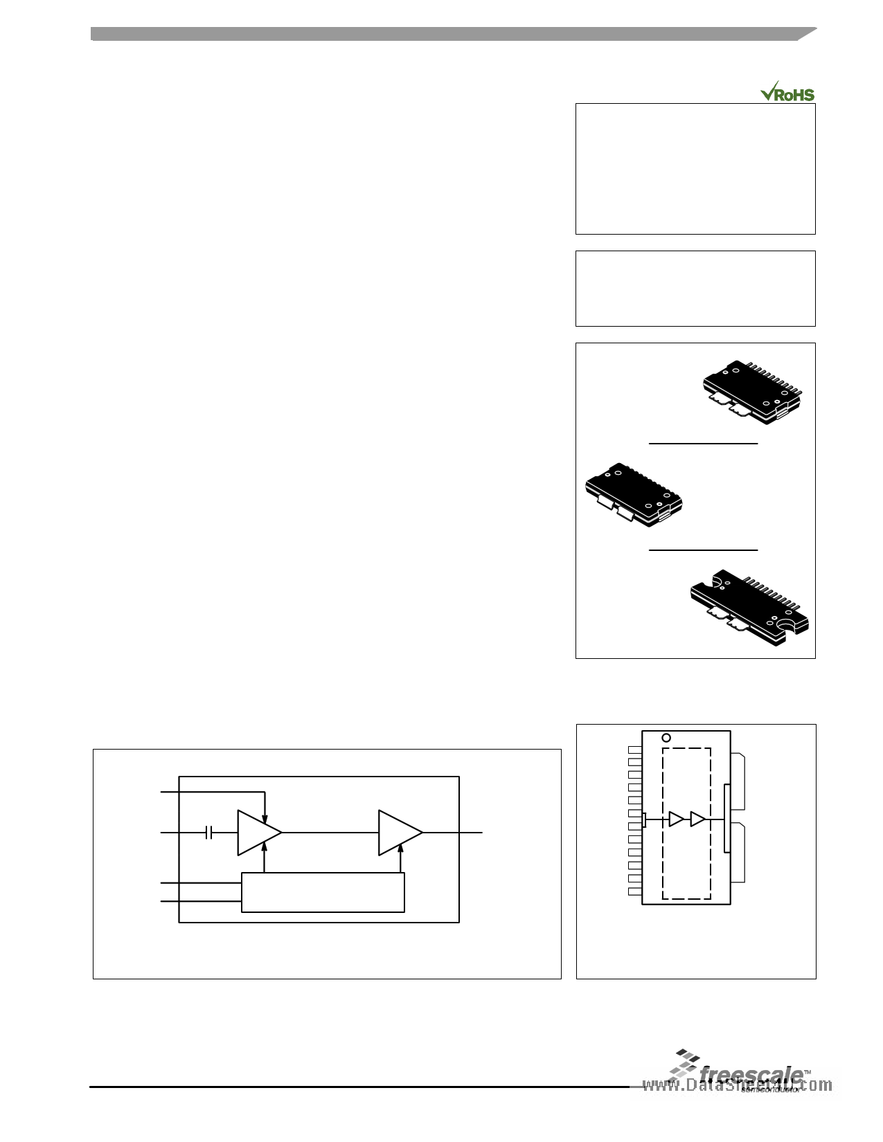
VDS1
RFin
VGS1
VGS2
Quiescent Current
Temperature Compensation (1)
RFout/VDS2
VDS1
VGS2
VGS1
NC
NC
RFin
RFin
NC
NC
VGS1
VGS2
VDS1
1
2
3
4
14
5
6
7
8
9 13
10
11
12
(Top View)
RFout /VDS2
RFout /VDS2
Note: Exposed backside of the package is
the source terminal for the transistors.
Figure 1. Functional Block Diagram
Figure 2. Pin Connections
1. Refer to AN1977, Quiescent Current Thermal Tracking Circuit in the RF Integrated Circuit Family and to AN1987, Quiescent Current
Control for the RF Integrated Circuit Device Family. Go to http://www.freescale.com/rf.
Select Documentation/Application Notes - AN1977 or AN1987.
© Freescale Semiconductor, Inc., 2008. All rights reserved.
RF Device Data
Freescale Semiconductor
MW7IC2750NR1 MW7IC2750GNR1 MW7IC2750NBR1
1
1 page 
VDD1
Z5
1
C2 C4
C6 2 NC
3 NC
RF
INPUT
Z1
Z2 Z3
4 NC
5 NC
6
www.datasheet4u.com
C1
7
8 NC
VGG1
VGG2
R1
R2
9 NC
10
11
Z4 12
C3 C5
C7
DUT
Quiescent Current
Temperature
Compensation
VDD2
Z12
14
Z6
13
Z11
C8 C13
C10 C12
Z7 Z8
Z9
RF
OUTPUT
Z10
C15
C11
C9 C14
Z1
Z2
Z3
Z4, Z5
Z6
Z7
0.662″ x 0.064″ Microstrip
1.530″ x 0.064″ Microstrip
0.126″ x 0.060″ Microstrip
0.771″ x 0.046″ Microstrip
0.192″ x 0.860″ Microstrip
0.280″ x 0.719″ Microstrip
Z8
Z9
Z10
Z11, Z12
PCB
0.417″ x 0.064″ Microstrip
1.137″ x 0.064″ Microstrip
0.293″ x 0.064″ Microstrip
0.615″ x 0.095″ Microstrip
Rogers RO4350B, 0.030″, εr = 3.66
Figure 3. MW7IC2750NR1(GNR1)(NBR1) Test Circuit Schematic
Table 6. MW7IC2750NR1(GNR1)(NBR1) Test Circuit Component Designations and Values
Part
Description
Part Number
C1
0.8 pF Chip Capacitor
ATC100B0R8BT500XT
C2, C3, C13, C14
10 μF, 50 V Chip Capacitors
GRM55DR61H106KA88B
C4, C5, C8, C9, C15
5.1 pF Chip Capacitors
ATC100B5R1CT500XT
C6, C7
1 μF, 100 V Chip Capacitors
GRM32ER72A105KA01L
C10, C11
0.2 pF Chip Capacitors
ATC100B0R2BT500XT
C12
0.5 pF Chip Capacitor
ATC100B0R5BT500XT
R1, R2
1 KΩ, 1/4 W Chip Resistors
CRCW12061001FKEA
Manufacturer
ATC
Murata
ATC
Murata
ATC
ATC
Vishay
RF Device Data
Freescale Semiconductor
MW7IC2750NR1 MW7IC2750GNR1 MW7IC2750NBR1
5
5 Page 
www.datasheet4u.com
Zo = 50 Ω
f = 2500 MHz
f = 2700 MHz
Zin
f = 2700 MHz
f = 2500 MHz
Zload
VDD = 28 Vdc, IDQ1 = 160 mA, IDQ2 = 550 mA, Pout = 8 W Avg.
f
MHz
Zin
W
Zload
W
2500
49.58 + j35.82
3.52 - j1.79
2525
50.78 + j36.71
3.46 - j1.82
2550
52.04 + j37.58
3.37 - j1.86
2575
53.39 + j38.45
3.24 - j1.88
2600
54.82 + j39.30
3.09 - j1.87
2625
56.35 + j40.14
2.94 - j1.84
2650
57.96 + j40.95
2.77 - j1.77
2675
59.68 + j41.74
2.60 - j1.66
2700
61.50 + j42.49
2.44 - j1.56
Zin = Device input impedance as measured from
gate to ground.
Zload = Test circuit impedance as measured
from drain to ground.
Device
Under Test
Output
Matching
Network
RF Device Data
Freescale Semiconductor
Z in Z load
Figure 16. Series Equivalent Source and Load Impedance
MW7IC2750NR1 MW7IC2750GNR1 MW7IC2750NBR1
11
11 Page | ||
| Páginas | Total 25 Páginas | |
| PDF Descargar | [ Datasheet MW7IC2750NR1.PDF ] | |
Hoja de datos destacado
| Número de pieza | Descripción | Fabricantes |
| MW7IC2750NR1 | RF Power Field Effect Transistors N-Channel Enhancement-Mode Lateral MOSFETs | Freescale Semiconductor |
| Número de pieza | Descripción | Fabricantes |
| SLA6805M | High Voltage 3 phase Motor Driver IC. |
Sanken |
| SDC1742 | 12- and 14-Bit Hybrid Synchro / Resolver-to-Digital Converters. |
Analog Devices |
|
DataSheet.es es una pagina web que funciona como un repositorio de manuales o hoja de datos de muchos de los productos más populares, |
| DataSheet.es | 2020 | Privacy Policy | Contacto | Buscar |