|
|
|
PDF ADCLK907 Data sheet ( Hoja de datos )
| Número de pieza | ADCLK907 | |
| Descripción | (ADCLK905 - ADCLK925) Ultrafast ECL Clock / Data Buffers | |
| Fabricantes | Analog Devices | |
| Logotipo | ||
Hay una vista previa y un enlace de descarga de ADCLK907 (archivo pdf) en la parte inferior de esta página. Total 16 Páginas | ||
|
No Preview Available !
www.DataSheet4U.com
FEATURES
95 ps propagation delay
7.5 GHz toggle rate
60 ps typical output rise/fall
60 fs random jitter (RJ)
On-chip terminations at both input pins
Extended industrial temperature range: −40°C to +125°C
2.5 V to 3.3 V power supply (VCC − VEE)
APPLICATIONS
Clock and data signal restoration and level shifting
Automated test equipment (ATE)
High speed instrumentation
High speed line receivers
Threshold detection
Converter clocking
GENERAL DESCRIPTION
The ADCLK905 (one input, one output), ADCLK907 (dual one
input, one output), and ADCLK925 (one input, two outputs) are
ultrafast clock/data buffers fabricated on the Analog Devices, Inc.,
proprietary XFCB3 silicon germanium (SiGe) bipolar process.
The ADCLK905/ADCLK907/ADCLK925 feature full-swing
emitter coupled logic (ECL) output drivers. For PECL (positive
ECL) operation, bias VCC to the positive supply and VEE to ground.
For NECL (negative ECL) operation, bias VCC to ground and
VEE to the negative supply.
The buffers offer 95 ps propagation delay, 7.5 GHz toggle rate,
10 Gbps data rate, and 60 fs random jitter (RJ).
The inputs have center tapped, 100 Ω, on-chip termination
resistors. A VREF pin is available for biasing ac-coupled inputs.
The ECL output stages are designed to directly drive 800 mV
each side into 50 Ω terminated to VCC − 2 V for a total
differential output swing of 1.6 V.
The ADCLK905/ADCLK907/ADCLK925 are available in
16-lead LFCSP packages.
Ultrafast SiGe
ECL Clock/Data Buffers
ADCLK905/ADCLK907/ADCLK925
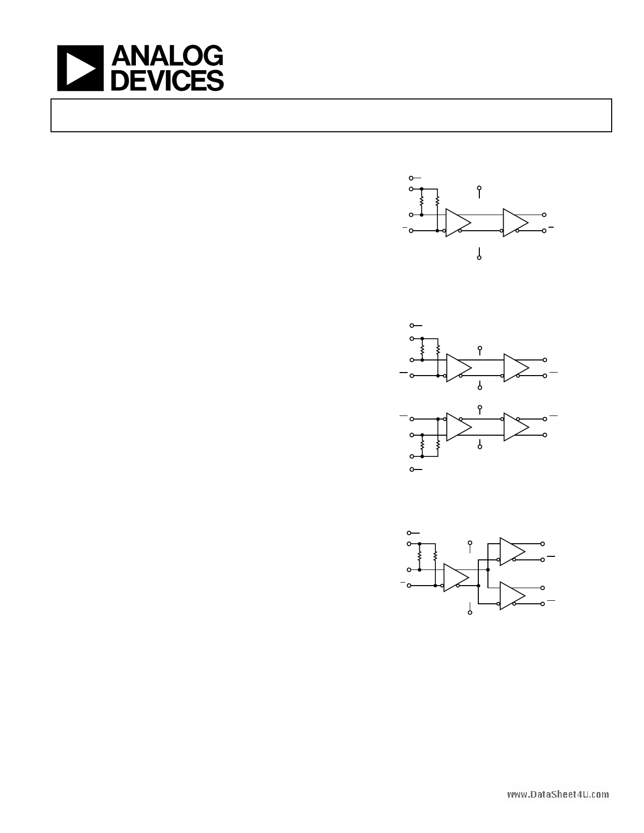
TYPICAL APPLICATION CIRCUITS
VREF
VT
VCC
DQ
DQ
VEE
Figure 1. ADCLK905 ECL 1:1 Clock/Data Buffer
VREF1
VT1
D1
D1
VCC
VEE
Q1
Q1
VEE
D2 Q2
D2 Q2
VCC
VT2
VREF2
Figure 2. ADCLK907 ECL Dual 1:1 Clock/Data Buffer
VREF
VT
VCC
Q1
Q1
D
D Q2
Q2
VEE
Figure 3. ADCLK925 ECL 1:2 Clock/Data Fanout Buffer
Rev. 0
Information furnished by Analog Devices is believed to be accurate and reliable. However, no
responsibility is assumed by Analog Devices for its use, nor for any infringements of patents or other
rights of third parties that may result from its use. Specifications subject to change without notice. No
license is granted by implication or otherwise under any patent or patent rights of Analog Devices.
Trademarksandregisteredtrademarksarethepropertyoftheirrespectiveowners.
One Technology Way, P.O. Box 9106, Norwood, MA 02062-9106, U.S.A.
Tel: 781.329.4700
www.analog.com
Fax: 781.461.3113
©2007 Analog Devices, Inc. All rights reserved.
1 page 
www.DataSheet4U.com
ABSOLUTE MAXIMUM RATINGS
Table 2.
Parameter
Supply Voltage
VCC − VEE
Input Voltage
D (D1, D2), D (D1, D2)
D1, D2, D1, D2 to VT Pin
(CML or PECL Termination)
D (D1, D2) to D (D1, D2)
Maximum Voltage on Output Pins
Maximum Output Current
Input Termination, VT to D (D1, D2), D (D1, D2)
Voltage Reference, VREF
Temperature
Operating Temperature Range, Ambient
Operating Temperature, Junction
Storage Temperature Range
Rating
6.0 V
VEE − 0.5 V to
VCC + 0.5 V
±40 mA
±1.8 V
VCC + 0.5 V
35 mA
±2 V
VCC − VEE
−40°C to +125°C
150°C
−65°C to +150°C
Stresses above those listed under Absolute Maximum Ratings
may cause permanent damage to the device. This is a stress
rating only; functional operation of the device at these or any
other conditions above those indicated in the operational
section of this specification is not implied. Exposure to absolute
maximum rating conditions for extended periods may affect
device reliability.
ADCLK905/ADCLK907/ADCLK925
THERMAL RESISTANCE
θJA is specified for the worst-case conditions, that is, a device
soldered in a circuit board for surface-mount packages.
Table 3. Thermal Resistance
Package Type
θJA
16-lead LFCSP
70
Unit
°C/W
ESD CAUTION
Rev. 0 | Page 5 of 16
5 Page 
www.DataSheet4U.com
APPLICATIONS INFORMATION
POWER/GROUND LAYOUT AND BYPASSING
The ADCLK905/ADCLK907/ADCLK925 buffers are designed
for very high speed applications. Consequently, high speed design
techniques must be used to achieve the specified performance.
It is critically important to use low impedance supply planes for
both the negative supply (VEE) and the positive supply (VCC) planes
as part of a multilayer board. Providing the lowest inductance
return path for switching currents ensures the best possible
performance in the target application.
It is also important to adequately bypass the input and output
supplies. A 1 μF electrolytic bypass capacitor should be placed
within several inches of each power supply pin to ground. In
addition, multiple high quality 0.001 μF bypass capacitors
should be placed as close as possible to each of the VEE and VCC
supply pins and should be connected to the GND plane with
redundant vias. High frequency bypass capacitors should be
carefully selected for minimum inductance and ESR. Parasitic
layout inductance should be strictly avoided to maximize the
effectiveness of the bypass at high frequencies.
OUTPUT STAGES
The specified performance can be achieved only by using proper
transmission line terminations. The outputs of the ADCLK905/
ADCLK907/ADCLK925 buffers are designed to directly drive
800 mV into 50 Ω cable or microstrip/stripline transmission
lines terminated with 50 Ω referenced to VCC − 2 V. The PECL
output stage is shown in Figure 25. The outputs are designed for
best transmission line matching. If high speed signals must be
routed more than a centimeter, either the microstrip or the
stripline technique is required to ensure proper transition times
and to prevent excessive output ringing and pulse width-
dependent propagation delay dispersion.
VCC
Q
Q
ADCLK905/ADCLK907/ADCLK925
OPTIMIZING HIGH SPEED PERFORMANCE
As with any high speed circuit, proper design and layout
techniques are essential to obtaining the specified performance.
Stray capacitance, inductance, inductive power and ground
impedances, or other layout issues can severely limit performance
and cause oscillation. Discontinuities along input and output
transmission lines can also severely limit the specified jitter
performance by reducing the effective input slew rate.
In a 50 Ω environment, input and output matching have a
significant impact on performance. The buffer provides internal
50 Ω termination resistors for both D and D inputs. The return
side should normally be connected to the reference pin provided.
The termination potential should be carefully bypassed, using
ceramic capacitors to prevent undesired aberrations on the
input signal due to parasitic inductance in the termination
return path. If the inputs are directly coupled to a source, care
must be taken to ensure the pins are within the rated input
differential and common-mode ranges.
If the return is floated, the device exhibits 100 Ω cross termination,
but the source must then control the common-mode voltage
and supply the input bias currents.
There are ESD/clamp diodes between the input pins to prevent
the application of excessive offsets to the input transistors. ESD
diodes are not optimized for best ac performance. When a
clamp is desired, it is recommended that appropriate external
diodes be used.
BUFFER RANDOM JITTER
The ADCLK905/ADCLK907/ADCLK925 are specifically
designed to minimize added random jitter over a wide input
slew rate range. Provided sufficient voltage swing is present,
random jitter is affected most by the slew rate of the input signal.
Whenever possible, excessively large input signals should be
clamped with fast Schottky diodes because attenuators reduce
the slew rate. Input signal runs of more than a few centimeters
should be over low loss dielectrics or cables with good high
frequency characteristics.
VEE
Figure 25. Simplified Schematic Diagram of
the ADCLK905/ADCLK907/ADCLK925 PECL Output Stage
Rev. 0 | Page 11 of 16
11 Page | ||
| Páginas | Total 16 Páginas | |
| PDF Descargar | [ Datasheet ADCLK907.PDF ] | |
Hoja de datos destacado
| Número de pieza | Descripción | Fabricantes |
| ADCLK905 | (ADCLK905 - ADCLK925) Ultrafast ECL Clock / Data Buffers | Analog Devices |
| ADCLK907 | (ADCLK905 - ADCLK925) Ultrafast ECL Clock / Data Buffers | Analog Devices |
| Número de pieza | Descripción | Fabricantes |
| SLA6805M | High Voltage 3 phase Motor Driver IC. |
Sanken |
| SDC1742 | 12- and 14-Bit Hybrid Synchro / Resolver-to-Digital Converters. |
Analog Devices |
|
DataSheet.es es una pagina web que funciona como un repositorio de manuales o hoja de datos de muchos de los productos más populares, |
| DataSheet.es | 2020 | Privacy Policy | Contacto | Buscar |