|
|
PDF NJG1135MD7 Data sheet ( Hoja de datos )
| Número de pieza | NJG1135MD7 | |
| Descripción | CDMA DUAL BAND LNA GaAs MMIC | |
| Fabricantes | NJR Corporation | |
| Logotipo |  |
|
Hay una vista previa y un enlace de descarga de NJG1135MD7 (archivo pdf) en la parte inferior de esta página. Total 20 Páginas | ||
|
No Preview Available !
www.DataSheet4U.com
NJG1135MD7
CDMA DUAL BAND LNA GaAs MMIC
! GENERAL DESCRIPTION
The NJG1135MD7 is a GaAs LNA MMIC designed for CDMA2000 dual
band (Cellular and PCS) application. The NJG1135MD7 has LNA
pass-through function to select high gain mode or low gain.
The NJG1135MD7 achieved high IIP3 and low noise figure at the high
gain mode, and low current consumption at the low gain mode.
An ultra-small and ultra-thin EQFN14-D7 package is adopted.
! PACKAGE OUTLINE
NJG1135MD7
! FEATURES
"Low voltage operation
"Low control voltage operation
+2.8V typ.
+1.8V min.
[LNA high gain mode]
"High input IP3
"High gain
"Low noise figure
+10dBm typ.
+8dBm typ.
+16dB typ.
1.4dB typ.
@ f=880MHz
@ f=1960MHz
@ f=880MHz / 1960MHz
@ f=880MHz / 1960MHz
[LNA low gain mode]
"Low current consumption
"High input IP3
" Ultra-small and ultra-thin package
30uA typ.
+19dBm typ. @ f=880MHz
+17dBm typ. @ f=1960MHz
EQFN14-D7 (Package size: 1.6x1.6x0.397mm typ., Lead and Halogen-Free)
! PIN CONFIGURATION
(Top View)
11 10 9
8
12 Cellular
7
13 PCS
6
14 5
Pin Connection
1. GND
2. VCTL2
3. VCTL1
4. GND
5. RFOUT1
6. RFOUT2
7. GND
8. GND
9. GND
10. GND
11. GND
12. RFIN2
13. RFIN1
14. GND
123 4
! TRUETH TABLE
“H”=VCTL(H), “L”=VCTL(L)
VCTL1 VCTL2
Cellular band
LNA Bypass
L L OFF ON
L H ON OFF
H L OFF ON
H H ON OFF
PCS band
LNA Bypass
OFF ON
OFF ON
ON OFF
ON OFF
Note: Specifications and description listed in this datasheet are subject to change without notice.
Ver. 2008-10-31
-1-
1 page 
www.DataSheet4U.com
! TERMINAL INFOMATION
No. SYMBOL
NJG1135MD7
DESCRIPTION
1 GND Ground terminal.
Control port 2. This terminal is set to more than +1.8V~+2.95V of logical high level
2 VCTL2 for high gain mode of cellular band LNA, and set to –0.3V~+0.3V of logical low
level for low gain mode of cellular band LNA.
Control port 1. This terminal is set to more than +1.8V~+2.95V of logical high level
3 VCTL1 for high gain mode of PCS band LNA, and set to –0.3V~+0.3V of logical low level
for low gain mode of PCS band LNA.
4 GND Ground terminal.
RF output terminal of PCS band signal. RF signal and DC power is input through
5 RFOUT1 external matching circuit connected to this terminal. External matching circuit and
DC blocking capacitor are required.
RF output terminal of cellular band signal. RF signal and DC power is input
6 RFOUT2 through external matching circuit connected to this terminal. External matching
circuit and DC blocking capacitor are required.
7 GND Ground terminal. This terminal is not connected with internal circuit.
8 GND Ground terminal.
9 GND Ground terminal. This terminal is not connected with internal circuit.
10 GND Ground terminal. This terminal is not connected with internal circuit.
11 GND Ground terminal.
RF input terminal of cellular band signal. RF signal is input through external
12 RFIN2 matching circuit connected to this terminal. A DC blocking capacitor is not
required.
RF input terminal of PCS band signal. RF signal is input through external
13 RFIN1 matching circuit connected to this terminal. A DC blocking capacitor is not
required.
14 GND Ground terminal. This terminal is not connected with internal circuit.
Notes:
1) Ground terminal (No.1, 4, 8, and 11) should be connected with the ground plane as close as possible
for good RF performance, because distance to GND makes parasitic inductance.
-5-
5 Page 
NJG1135MD7
www.DataSheet4U.com
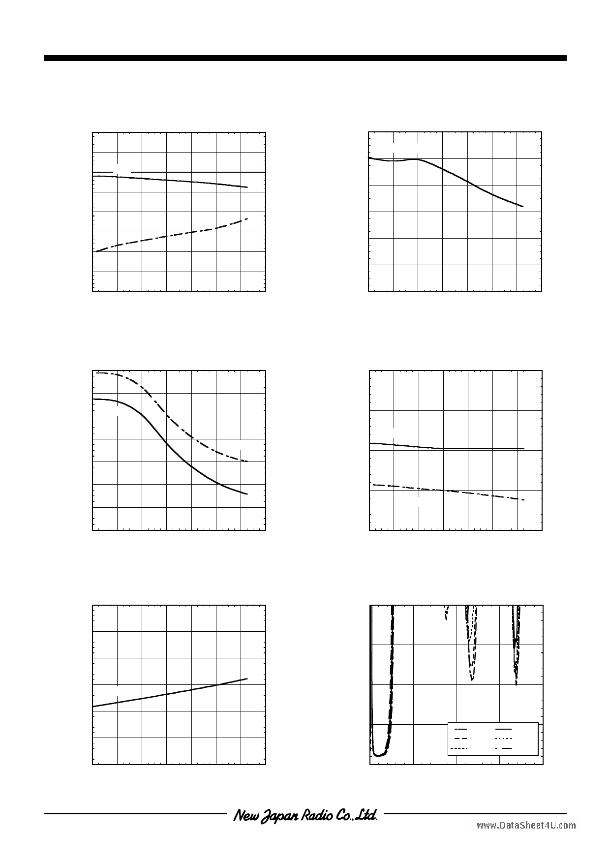
! ELECTRICAL CHARACTERISTICS (Cellular Band: LNA Low Gain Mode)
(General Conditions: VDD=2.8V, VCTL1=0V, VCTL2=2.8V, fRF=880MHz, Zs=Zl=50Ω, with application circuit)
Gain, NF vs. Temperature
P-1dB(IN) vs. Temperature
f=880MHz
08
f=880MHz
16
-1
-2 Gain
-3
7 P-1dB(IN)
14
6
12
5
-4 4 10
-5
NF 3
8
-6 2
6
-7 1
-8
-40 -20
0 20 40 60
Temperature (oC)
0
80 100
4
-40 -20
0 20 40 60 80 100
Temperature (oC)
OIP3, IIP3 vs. Temperature
f1=880MHz, f2=f1+100kHz, Pin=-12dBm
28 28
26
24 OIP3
26
24
22 IIP3 22
20 20
18 18
16 16
14
-40 -20
0 20 40 60
Temperature (oC)
14
80 100
IDD vs. Temperature
RF off
60
50
40
30
IDD
20
10
0
-40 -20
0 20 40 60
Temperature (oC)
80 100
VSWRi, VSWRo vs. Temperature
f=880MHz
3
2.5
VSWRi
2
1.5
VSWRo
1
-40 -20
0 20 40 60 80 100
Temperature (oC)
K factor vs. frequency
f=50M~20GHz
20
15
10
5
0
0
Ta=-40oC
Ta=-20oC
Ta=0oC
Ta=25oC
Ta=60oC
Ta=85oC
5 10 15 20
frequency (GHz)
- 11 -
11 Page | ||
| Páginas | Total 20 Páginas | |
| PDF Descargar | [ Datasheet NJG1135MD7.PDF ] | |
Hoja de datos destacado
| Número de pieza | Descripción | Fabricantes |
| NJG1135MD7 | CDMA DUAL BAND LNA GaAs MMIC | NJR Corporation |
| Número de pieza | Descripción | Fabricantes |
| SLA6805M | High Voltage 3 phase Motor Driver IC. |
Sanken |
| SDC1742 | 12- and 14-Bit Hybrid Synchro / Resolver-to-Digital Converters. |
Analog Devices |
|
DataSheet.es es una pagina web que funciona como un repositorio de manuales o hoja de datos de muchos de los productos más populares, |
| DataSheet.es | 2020 | Privacy Policy | Contacto | Buscar |
