|
|
|
PDF SYS88000RKX-10 Data sheet ( Hoja de datos )
| Número de pieza | SYS88000RKX-10 | |
| Descripción | 8M x 8 SRAM MODULE | |
| Fabricantes | MOSAIC | |
| Logotipo | ||
Hay una vista previa y un enlace de descarga de SYS88000RKX-10 (archivo pdf) en la parte inferior de esta página. Total 7 Páginas | ||
|
No Preview Available !
www.DataSheet4U.com
8M x 8 SRAM MODULE
SYS88000RKX - 70/85/10/12
Issue 1.5: April 2001
Description
The SYS88000RKX is a plastic 64Mbit Static RAM
Module housed in a standard 38 pin Single In-Line
package organised as 8M x 8 with access times of
85,100, or 120 ns.
The module is constructed using sixteen 512Kx8 SRAMs
in TSOPII packages mounted onto both sides of an FR4
epoxy substrate. This offers an extremely high PCB
packing density.
The device is offered in standard and low power versions,
with the -L module having a low voltage data retention
mode for battery backed applications. On board buffering
is provided to reduce output capacitance.
Note: CS and OE on the module, should be used
with care to avoid on and off board bus contention.
Features
• Access Times of 85/100/120 ns.
• Low Power Disapation:
Operating
935 mW (Max.)
Standby -L Version 11 mW (Max.)
• 5 Volt Supply ± 10%.
• Completely Static Operation.
• Equal Access and Cycle Times.
• Low Voltage VCC Data Retention.
• On-board Decoding & Capacitors.
• 38 Pin Single-In-Line package.
• Upgrade from SYS84000RKX (32Mbit).
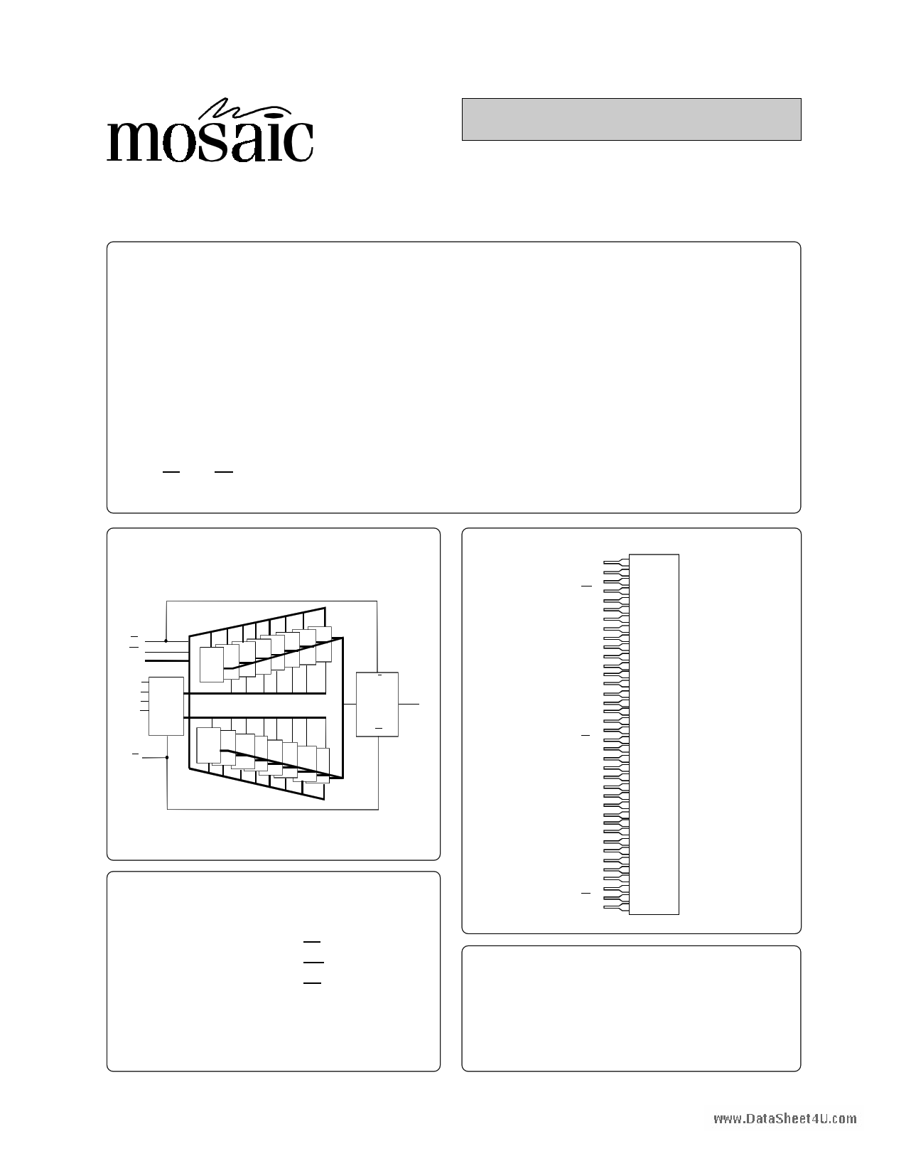
Block Diagram
OE
WE
A0 - A18
A19
A20
A21 4 TO 16
A22 DECODER
512K X 8
SRAM
512K X 8
SRAM
CS
D0 - D7
T/R
BI-DIRECTIONAL
DRIVERS D0 - D7
B0~7 A0~7
74FCT245
OE
Pin Functions
Address Inputs
Data Input/Output
Chip Select
Write Enable
Output Enable
No Connect
Power (+5V)
Ground
A0 ~ A22
D0 ~ D7
CS
WE
OE
NC
VCC
GND
Pin Definition
A22
A20
Vcc
WE
D2
D3
D0
A1
A2
A3
A4
GND
D5
A10
A11
A5
A13
A14
A19
CS
A15
A16
A12
A18
A6
D1
GND
A0
A7
A8
A9
D7
D4
D6
A17
Vcc
OE
A21
1
2
3
4
5
6
7
8
9
10
11
12
13
14
15
16
17
18
19
20
21
22
23
24
25
26
27
28
29
30
31
32
33
34
35
36
37
38
Package Details
Plastic 38 pin Single-In-Line (SIP)
1 page 
SYS88000RKX - 85/10/12
ISSUE 1.5 : April 2001
Read Cycle Timing Waveform (1,2)
www.DataSheet4U.com
Address
t RC
t AA
OE
CS
Dout
t OE
t OLZ
t ACS
t CLZ (4,5)
t OH
tOHZ (3)
Data Valid
tCHZ (3,4,5)
Don't
care.
AC Read Characteristics Notes
(1) WE is High for Read Cycle.
(2) All read cycle timing is referenced from the last valid address to the first transition address.
(3) tCHZ and tOHZ are defined as the time at which the outputs achieve open circuit conditions and are not
referenced to output voltage levels.
(4) At any given temperature and voltage condition, tCHZ (max) is less than tCLZ (min) both for a given module
and from module to module.
(5) These parameters are sampled and not 100% tested.
Write Cycle No.1 Timing Waveform(1,4)
Address
OE
CS
WE
Dout
Din
tWC
t AS(6)
t AW
t CW
t WR(7)
t OHZ(3,9)
High-Z
Don't
Care
t WP(2)
High-Z
tOW
t DW
t DH
Data Valid
(8)
5
5 Page | ||
| Páginas | Total 7 Páginas | |
| PDF Descargar | [ Datasheet SYS88000RKX-10.PDF ] | |
Hoja de datos destacado
| Número de pieza | Descripción | Fabricantes |
| SYS88000RKX-10 | 8M x 8 SRAM MODULE | MOSAIC |
| SYS88000RKX-12 | 8M x 8 SRAM MODULE | MOSAIC |
| Número de pieza | Descripción | Fabricantes |
| SLA6805M | High Voltage 3 phase Motor Driver IC. |
Sanken |
| SDC1742 | 12- and 14-Bit Hybrid Synchro / Resolver-to-Digital Converters. |
Analog Devices |
|
DataSheet.es es una pagina web que funciona como un repositorio de manuales o hoja de datos de muchos de los productos más populares, |
| DataSheet.es | 2020 | Privacy Policy | Contacto | Buscar |