|
|
|
PDF DEI1016 Data sheet ( Hoja de datos )
| Número de pieza | DEI1016 | |
| Descripción | Arinc 429 Transceiver | |
| Fabricantes | Device Engineering | |
| Logotipo | ||
Hay una vista previa y un enlace de descarga de DEI1016 (archivo pdf) en la parte inferior de esta página. Total 13 Páginas | ||
|
No Preview Available !
Devicewww.DataSheet4U.com
Engineering
Incorporated
430 S. Rockford Dr.
Tempe, AZ 85281
Phone: (480) 303-0822
Fax: (480) 303-0824
E-mail: [email protected]
DEI 1016
ARINC 429 Transceiver
Features
• Two Receivers and One Transmitter
• Harris/Holt/Raytheon Pin for Pin Replacement
• Wraparound Self-Test mode
• Word length of 25 or 32 bits
• Parity Status and generation of Receive and Transmit Words
• 8 Word Transmitter buffer
• Low Power CMOS processing
• Supports multiple ARINC data busses: 429, 571, 575, 706.
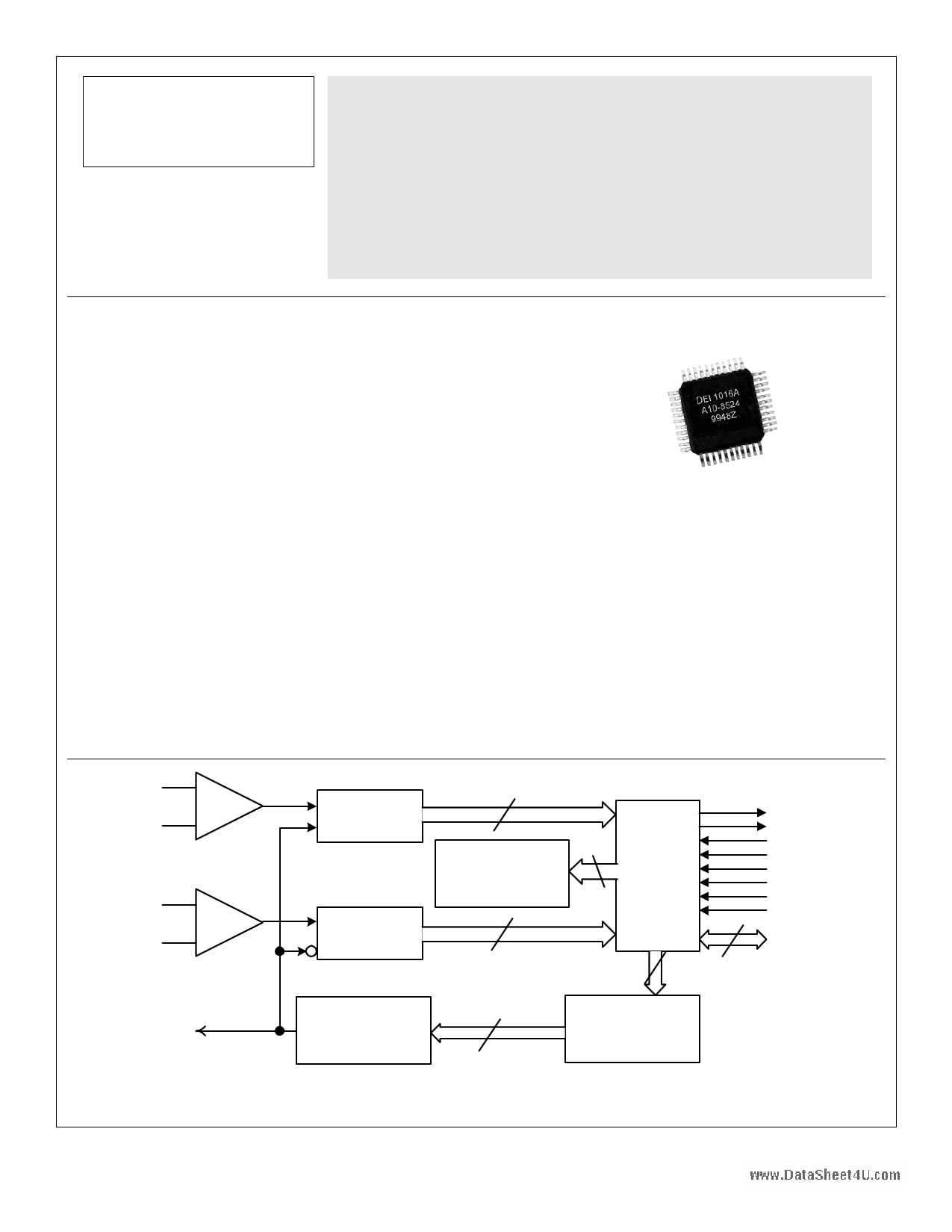
General Description:
The DEI 1016 provides an interface between a standard avionics type serial digital data bus and a 16-bit-wide
digital data bus. The interface circuit consists of a single channel transmitter with an 8X32 bit buffer, two inde-
pendent receive channels, and a host programmable control register to select operating options. The two re-
ceiver channels operate identically, each providing a direct electrical interface to an ARINC data bus.
The transmitter circuit contains an 8 word by 32 bit buffer memory and control logic which allows the host to
write a block of data into the transmitter. The block of data is transmitted automatically by enabling the trans-
mitter with no further attention by the host computer. Data is transmitted in TTL format on the D0(A)/D0(B) out-
put pins. The signal format is compatible with DEI’s extensive line of ARINC 429 Line drivers for easy connec-
tion to the ARINC data bus.
ARINC 429
Receive 0
ARINC 429
Receive 1
ARINC 429
Transmit
© Device Engineering Inc.
Tempe, Arizona
Receive
Decoder
Receive
Decoder
Transmit
Encoder
32 bit
Control
Register
32 bit
32 bit
16 bit
Host
Interface
32 bit
16 bit
/DR1or/DR2
TXR
/OE1 or /OE2
/LD1 or /LD2
ENTX
/LDCW
/DBCEN
/MR
DATA BUS
TX FIFO
8 Words X 32 Bits
Figure 1: DEI1016 Block Diagram
Page 1 of 13
DEI1016 Rev. C
July 20, 2000
1 page 
www.DDaatatSaheFeot4rUm.coamt:
The ARINC serial data is shuffled and formatted into two 16 bit words (WORD1 and WORD2) used by the bi-
directional data bus interface. Figure 2 shows the mapping between the 32 bit ARINC serial data and the two
data words. Figure 3 describes the mapping for the 25 bit serial word used when control register bit WLSEL is
set to logic “1”.
32 Bit ARINC Serial Data Format (Bit 1 is Transmitted First)
FUNCTION
SSM
DATA
S/D
or
DATA
LABEL
BIT 32 31 30 29 28 27 26 25 24 23 22 21 20 19 18 17 16 15 14 13 12 11 10 9 8 7 6 5 4 3 2 1
BIT 15 14 13 12 11 10 9 8 7 6 5 4 3 2 1 0 15 14 13 12 11 10 9 8 7 6 5 4 3 2 1 0
FUNCTION
DATA
DATA
S/D
or
DATA
SSM
LABEL
Word 2 Format
Word 1 Format
Figure 2: Mapping of Serial Data to/from Word 1 and Word 2 in 32 bit format.
25 Bit ARINC Serial Data Format (Bit 1 is Transmitted First)
FUNCTION
DATA
LABEL
BIT 25 24 23 22 21 20 19 18 17 16 15 14 13 12 11 10 9 8 7 6 5 4 3 2 1
BIT 15 14 13 12 11 10 9 8 7 6 5 4 3 2 1 0 15 14 13 12 11 10 9 8 7 6 5 4 3 2 1 0
FUNCTION
DATA
NOT USED
LABEL
Word 2 Format
Word 1 Format
Figure 3: Mapping of Serial Data to/from Word 1 and Word 2 in 25 bit format.
© Device Engineering Inc.
Tempe, Arizona
Page 5 of 13
DEI1016 Rev. C
July 20, 2000
5 Page 
www.SDaetraSiahel eItn4Ut.ecormface:
The DEI1016 consits of two receive channels and one
transmit channel. Each receive channel operates inde-
pendently of each other and the transmitter. The re-
ceive data is asynchronous to the transmitter data and
can also be at a different data rate than the transmitter.
Transmitter
The transmitter clock is free running and in phase with
the transmitter data. The transmitter data (DO(A) and
DO(B)) are TTL level signals. There are always at least
4 null bits between data words. An external ARINC line
driver is required to interface the transmitter to the
ARINC serial data bus. See ARINC 429 LINE DRIV-
ERS below.
Receiver
The receiver signals (DI(A) and DI(B)) are differential,
bipolar, return-to-zero logic signals. The ARINC chan-
nels can be connected directly to the receiver with no
external components.
ARINC 429 Line Driver
Device Engineering offers a complete line of ARINC
line drivers that support the ARINC 429, 571, and 575
standards. Please visit our website at http://www.deiaz.
com to view and download data sheets for our line driv-
ers.
N/C
/DR1
/DR2
SEL
/OE1
/OE2
D15
D14
D13
D12
D11
44 43 42 41 40 39 38 37 36 35 34
1 33
2 32
3 31
4
DEI1016A
30
5 29
6
44 - Pin
28
7
Plastic
27
8
PQFP
26
9 25
10 24
11 23
12 13 14 15 16 17 18 19 20 21 22
N/C
N/C
/LDCW
ENTX
DO(B)
DO(A)
TXR
/LD2
/LD1
D0
D1
Figure 12: DEI1016A Pin-Out
V
DD
1
DI1(A) 2
DI1(B) 3
DI2(A) 4
DI2(B) 5
/DR1 6
/DR2 7
SEL 8
/OE1 9
/OE2 10
D15 11
D14 12
D13 13
D12 14
D11 15
D10 16
D9 17
D8 18
D7 19
D6 20
DEI1016
40 Pin Ceramic
Side Brazed
DIP
and
DEI1016C
40 Pin Plastic
DIP
40 /DBCEN
39 /MR
38 TXCK
37 1MCK
36 N/C
35 N/C
34 /LDCW
33 ENTX
32 DO(B)
31 DO(A)
30 TXR
29 /LD2
28 /LD1
27 D0
26 D1
25 D2
24 D3
23 D4
22 D5
21 GND
Figure 11: DEI1016 and DEI1016C Pin-Out
N/C
/DR1
/DR2
SEL
/OE1
/OE2
D15
D14
D13
D12
D11
6 5 4 3 2 1 44 43 42 41 40
7 39
8 38
9 37
10
DEI1016B
36
11 35
12 44 - Pin 34
13 Plastic 33
14 PLCC 32
15 31
16 30
17 29
18 19 20 21 22 23 24 25 26 27 28
N/C
N/C
/LDCW
ENTX
DO(B)
DO(A)
TXR
/LD2
/LD1
D0
D1
Figure 13: DEI1016B Pin-Out
© Device Engineering Inc.
Tempe, Arizona
Page 11 of 13
DEI1016 Rev. C
July 20, 2000
11 Page | ||
| Páginas | Total 13 Páginas | |
| PDF Descargar | [ Datasheet DEI1016.PDF ] | |
Hoja de datos destacado
| Número de pieza | Descripción | Fabricantes |
| DEI1016 | Arinc 429 Transceiver | Device Engineering |
| DEI1016 | Arinc 429 Transceiver | Device Engineering |
| DEI1016A | Arinc 429 Transceiver | Device Engineering |
| DEI1016B | Arinc 429 Transceiver | Device Engineering |
| Número de pieza | Descripción | Fabricantes |
| SLA6805M | High Voltage 3 phase Motor Driver IC. |
Sanken |
| SDC1742 | 12- and 14-Bit Hybrid Synchro / Resolver-to-Digital Converters. |
Analog Devices |
|
DataSheet.es es una pagina web que funciona como un repositorio de manuales o hoja de datos de muchos de los productos más populares, |
| DataSheet.es | 2020 | Privacy Policy | Contacto | Buscar |