|
|
PDF L6713A Data sheet ( Hoja de datos )
| Número de pieza | L6713A | |
| Descripción | 2/3 phase controller | |
| Fabricantes | STMicroelectronics | |
| Logotipo |  |
|
Hay una vista previa y un enlace de descarga de L6713A (archivo pdf) en la parte inferior de esta página. Total 30 Páginas | ||
|
No Preview Available !
www.DataSheet4U.com
L6713A
2/3 phase controller with embedded drivers for Intel VR10, VR11
and AMD 6 bit CPUs
Features
■ Load transient boost LTB Technology™ to
minimize the number of output capacitors
(patent pending)
■ Dual-edge asynchronous PWM
■ Selectable 2 or 3 phase operation
■ 0.5 % output voltage accuracy
■ 7/8 bit programmable output up to 1.60000 V -
Intel VR10.x, VR11 DAC
■ 6 bit programmable output up to 1.5500 V -
AMD 6 bit DAC
■ High current integrated gate drivers
■ Full differential current sensing across inductor
■ Embedded VRD thermal monitor
■ Differential remote voltage sensing
■ Dynamic VID management
■ Adjustable voltage offset
■ Low-side-less startup
■ Programmable soft-start
■ Programmable over voltage protection
■ Preliminary over voltage protection
■ Programmable over current protection
■ Adjustable switching frequency
■ Output enable
■ SS_END / PGOOD signal
■ TQFP64 10x10 mm package with exposed pad
Applications
■ High current VRD for desktop CPUs
■ Workstation and server CPU power supply
■ VRM modules
Table 1. Device summary
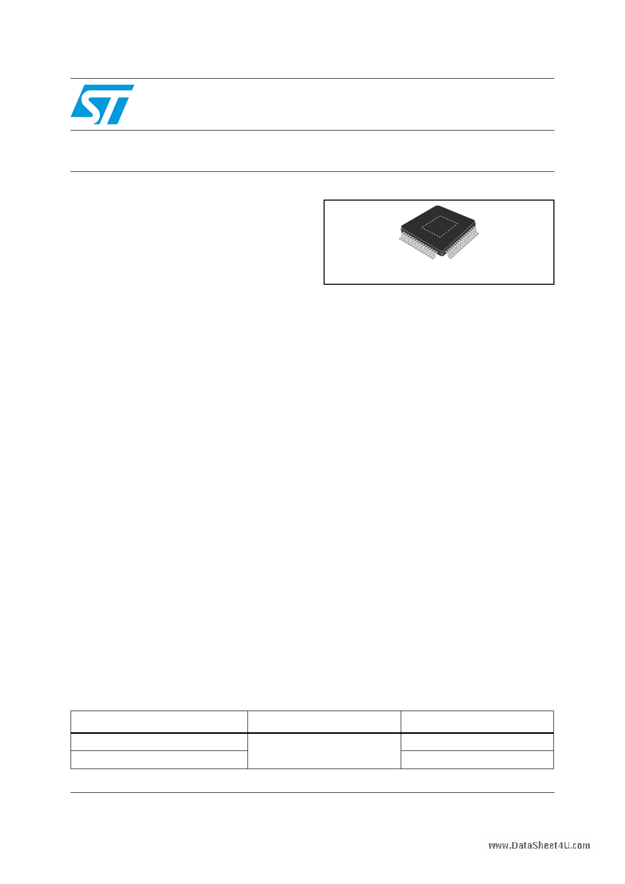
TQFP64 (Exposed pad)
Description
L6713A implements a two/three phase step-down
controller with 180º/120º phase-shift between
each phase with integrated high current drivers in
a compact 10x10 mm body package with exposed
pad.The 2 or 3 phase operation can be easily
selected through PHASE_SEL pin.
Load transient boost LTB Technology™ (patent
pending) reduces system cost by providing the
fastest response to load transition therefore
requiring less bulk and ceramic output capacitors
to satisfy load transient requirements.
LTB Technology™ can be disabled and in this
condition the device works as a dual-edge
asynchronous PWM.
The device embeds selectable DACs: the output
voltage ranges up to 1.60000 V (both Intel VR10.x
and VR11 DAC) or up to 1.5500 V (AMD 6BIT
DAC) managing D-VID with ± 0.5% output voltage
accuracy over line and temperature variations.
The controller assures fast protection against load
over current and under / over voltage (in this last
case also before UVLO). In case of over-current
the device turns off all MOSFET and latches the
condition.
System thermal monitor is also provided allowing
system protection from over-temperature
conditions.
Order codes
Package
Packaging
L6713A
L6713ATR
TQFP64 (Exposed pad)
Tube
Tape and reel
August 2008
Rev 3
1/64
www.st.com
64
1 page 
www.DataSLh6e7et143UA.com
1 Block diagram
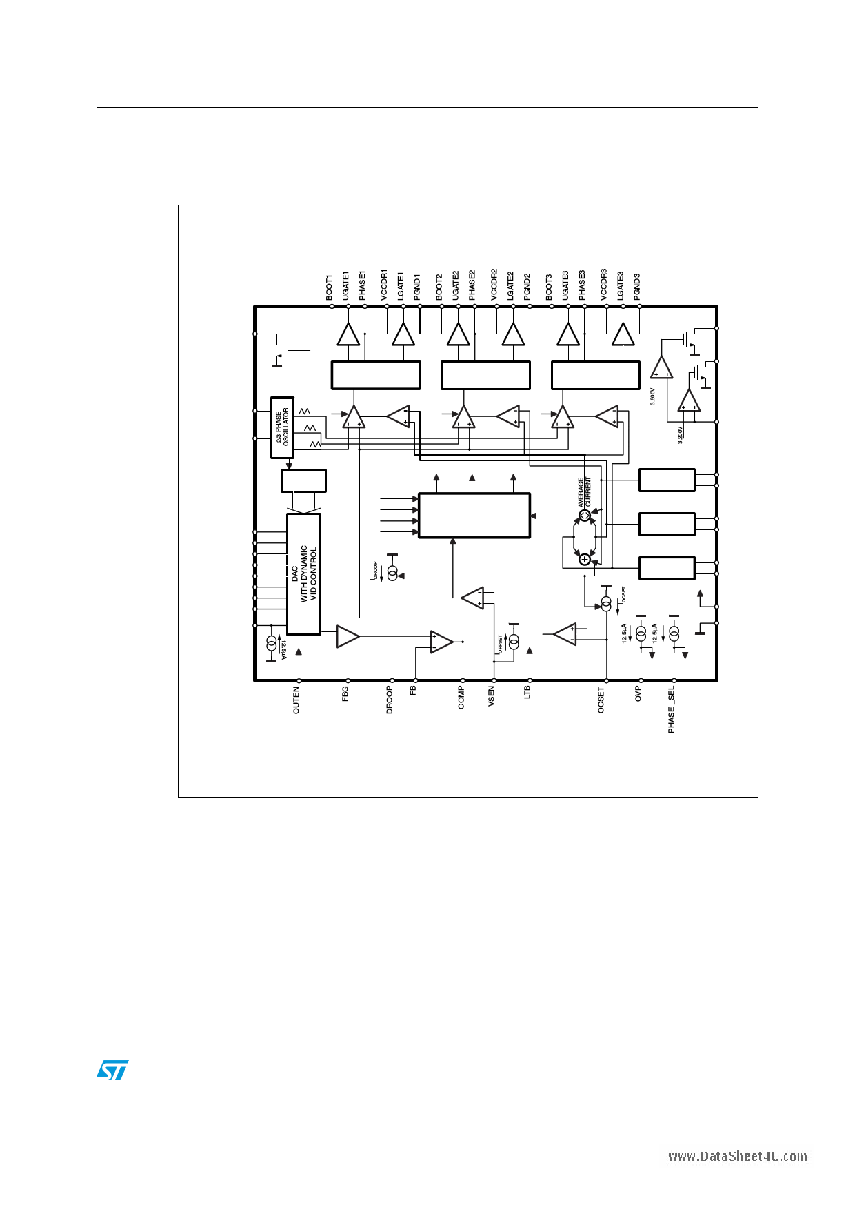
Figure 1. Block diagram
Block diagram
SS_END / PGOOD
OSC / FAULT
SS/ LTBG/ AMD
VID0
VID1
VID2
VID3
VID4
VID5
VID6
VID7 / D-VID
VID_SEL
HS1 LS1
LOGIC PWM
ADAPTIVE ANTI
CROSS CONDUCTION
CURRENT SHARING
CORRECTION
LTB
PWM1
HS2 LS2
LOGIC PWM
ADAPTIVE ANTI
CROSS CONDUCTION
CURRENT SHARING
CORRECTION
LTB
PWM2
HS3 LS3
LOGIC PWM
ADAPTIVE ANTI
CROSS CONDUCTION
LTB
CURRENT SHARING
CORRECTION
PWM3
VR_HOT
VR_FAN
TM
DIGITAL
SOFT START
PWM1
PWM2
PWM3
VCC
VCCDR
OUTEN
SSOSC/AMD
L6713A
CONTROL LOGIC
AND PROTECTIONS
OCP
OUTEN
GND DROP
RECOVERY
VREF
ERROR
AMPLIFIER
TOTAL DELIVERED CURRENT
+175mV / 1.800V / OVP
OVP
COMPARATOR
TO OCP
+.1240V
OCP
LTB COMPARATOR
CH1 CURRENT
READING
CS1-
CS1+
CH2 CURRENT
READING
CS2-
CS2+
CH3 CURRENT
READING
VCC
CS3-
CS3+
VCC
SGND
OVP
PHASE_SEL
5/64
5 Page 
www.DataSLh6e7et143UA.com
Pin settings
Table 2. Pin description (continued)
N° Pin
Function
Channel 2 LS driver supply.
It must be connected to others VCCDRx pins also when using 2-phase
56 VCCDR2 operation.
LS driver supply can range from 5 Vbus up to 12 Vbus, filter with 1 µF MLCC
cap vs. PGND2.
Channel 3 LS driver supply.
57 VCCDR3 It must be connected to others VCCDRx pins.
LS driver supply can range from 5 Vbus up to 12 Vbus, filter with 1 µF MLCC
cap vs. PGND3.
58
LGATE3
Channel 3 LS driver output. A small series resistor helps in reducing device-
dissipated power.
59 PGND3 Channel 3 LS driver return path. Connect to power ground plane.
60 PGND1 Channel 1 LS driver return path. Connect to power ground plane.
61
LGATE1
Channel 1 LS driver output. A small series resistor helps in reducing device-
dissipated power.
Channel 1 LS driver supply.
62 VCCDR1 It must be connected to others VCCDRx pins.
LS driver supply can range from 5 Vbus up to 12 Vbus, filter with 1 µF MLCC
cap vs. PGND1.
Channel 1 HS driver return path.
63 PHASE1 It must be connected to the HS1 MOSFET source and provides return path for
the HS driver of channel 1.
64 N.C. Not internally connected.
Thermal pad connects the silicon substrate and makes good thermal contact
PAD
Thermal with the PCB to dissipate the power necessary to drive the external MOSFETs.
pad
Connect to the PGND plane with several VIAs to improve thermal conductivity.
11/64
11 Page | ||
| Páginas | Total 30 Páginas | |
| PDF Descargar | [ Datasheet L6713A.PDF ] | |
Hoja de datos destacado
| Número de pieza | Descripción | Fabricantes |
| L6713A | 2/3 phase controller | STMicroelectronics |
| Número de pieza | Descripción | Fabricantes |
| SLA6805M | High Voltage 3 phase Motor Driver IC. |
Sanken |
| SDC1742 | 12- and 14-Bit Hybrid Synchro / Resolver-to-Digital Converters. |
Analog Devices |
|
DataSheet.es es una pagina web que funciona como un repositorio de manuales o hoja de datos de muchos de los productos más populares, |
| DataSheet.es | 2020 | Privacy Policy | Contacto | Buscar |
